Pages Menu
Categories Menu

Posted in Featured Products

Advantest Rolls Out Thermal Control Products for MPT3000 Solid-State Drive Test Platform

Independent Thermal Control Board and Engineering Thermal Chamber Targeting Early SSD Product Development Stages with Per DUT Thermal Control

In August, Advantest announced two new additions to its MPT3000 solid-state drive (SSD) test platform. The Independent Thermal Control (ITC) device interface boards (DIBs) and Engineering Thermal Chamber (ETC) target early engineering adoption of the MPT3000 by enabling efficient, small-batch engineering, quality assurance and early test development for SSD devices.

Advanced computing standards, such as PCI Express fifth-generation (PCIe Gen 5), enable higher-speed SSD devices with greatly expanded bandwidth for use in advanced data centers and other demanding storage applications. These faster, higher-capacity devices must be characterized and tested in thermal environments that accurately replicate operating temperatures.

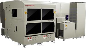
Designed for device test qualification and validation, the ETC is integrated into the MPT3000ES3 test system to handle the highest-power PCIe Gen 5 DUTs. The unit enables accurate environmental temperature control within the chamber from -10 to 85°C, utilizing air flow to accurately condition up to 32 4-lane DUTs. The ETC is well suited for characterizing small batches of DUTs at a set temperature within the range stated.

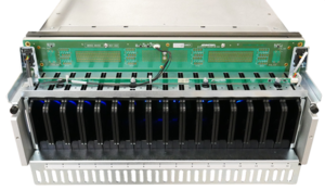
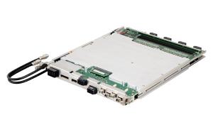
Created for high-volume production test and qualification, the MPT3000HVM3 test systems support ITC DIBs, allowing the user to accurately set and maintain a constant drive temperature. Using active temperature feedback from the DUT, the fan speed is controlled to maintain a constant DUT temperature. This is an improvement from standard DIBs, which supply constant cooling air and allow the DUT temperature to fluctuate with the wattage of the test cycle. ITC DIBs feature air channels on either side of the DUT to maintain a constant DUT temperature on all DUTs, even during asynchronous testing cycles.


Read More

Posted in Featured Products

Advantest Ships 10,000th V93000 SoC Test System

Advantest recently announced that it shipped its 10,000th V93000 system-on-chip (SoC) test system to longtime customer Infineon Technologies, the world’s number one automotive semiconductor supplier. The milestone system is a V93000 configuration developed to address the diverse test needs of power, analog, microcontroller and sensor ICs used in automotive and microcontroller applications. Ever-increasing semiconductor content in today’s automobiles is creating a pressing need for the V93000’s combination of advanced test capabilities and leading cost-of-test savings.

“Advantest’s V93000 tester has proven to be a highly effective digital, power and mixed-signal tester for us. The partnership with Advantest has helped to enable fast time-to-market while hitting our challenging cost-of-test targets,” said Ralf Schuster, senior vice president, Test and Automation Technologies, Infineon. “We have worked with Advantest for many years, and we are pleased to be the recipient of the 10,000th V93000 shipment.”

In the more than two decades since its introduction, the flexible, scalable V93000 has become Advantest’s flagship SoC test platform. The company offers a wide range of V93000 options together with complementary test instruments – including universal analog and digital test cards, RF instrumentation and mixed-signal cards, and best-in-class DPS and floating-power VI cards – as well as the user-friendly SmarTest system software environment. The newest V93000 offering is the EXA Scale generation system for testing a wide range of devices, from current and future generations of low-cost Internet of Things (IoT) chips to high-end automotive devices, highly integrated multicore processors, and advanced digital ICs up to the exascale performance class.

Read More

Posted in Featured Products

Advantest Targets High-Numerical Aperture (NA) EUV Photomasks with Industry-Leading E3650 MVM-SEM

The market for photomasks used in high-numerical-aperture (NA) extreme-ultraviolet (EUV) lithography is growing quickly as chipmakers seek patterning solutions for sub-5nm masks. To take advantage of this growth, Advantest is leveraging the capabilities of its proven E3650 multi-vision metrology scanning electron microscope (MVM-SEM®). Since its introduction in 2018, the E3650 has become the standard for EUV mask measurement, making the system well-positioned for the high-NA market.

Highly advanced masks are vital for the development of complex chips that consume less power, such as those implemented in mobile phones. EUV lithography was developed to accommodate the printing of sub-7nm mask features, which 193nm-wavelength lithography systems are unable to handle. However, single-pattern EUV reaches its limit at around the 5nm node. At 3nm and beyond, high-NA EUV, which enables scaling down to the angstrom level, offers a simpler approach than costlier and more complex EUV double patterning. According to ASML, “High-NA EUV will bring multiple benefits to the semiconductor market such as reduction of process complexity, yield improvement, higher resolution enabling printability of smaller features at increased density, and cost of technology reduction.”1

The E3650 MCM-SEM uses Advantest’s proprietary electron beam scanning technology to measure fine pattern dimensions on photomasks with high precision and stability. The system’s higher throughput enables massive measurement required by more complex patterning and an increased number of masks due to multiple patterning. Key features include fast move-acquire-measure (MAM) time, large field measurement, long-term stability of critical dimension (CD) measurements, design-based metrology support and 3D observation.

“The E5620 has proven its effectiveness in measuring masks for both 193nm and EUV lithography, delivering improvements in accuracy and throughput compared to earlier models in the E36XX series. These capabilities enable enhanced analysis as well as more efficient mass production of photomasks,” said Stuart Ainslie, senior director of business development, Advantest Europe. “Through its combination of unique features and our stellar global support, the E3650 has become the standard solution for measuring EUV masks. We look forward to capitalizing on this success in the high-NA EUV space.”

To learn more about the E3650, click here.

  1. “High NA EUV: development towards introduction at the customer,” SPIE Advanced Lithography and Patterning Conference, Feb. 2023


Read More

Posted in Featured Products

New AI-Powered Software Solution Accelerates Yield Improvement Throughout IC Engineering and Production

Advantest’s new yield-improvement solution leverages artificial intelligence (AI) to expedite identifying the root causes of yield loss and increasing the efficiency of analyzing test results. The innovative and scalable Advantest Cloud Solutions Engineering AI Studio for Yield Improvement (ACS EASYTM) can increase the productivity of both device engineering and production operations for a wide range of users, from chip designers to outsourced semiconductor assembly and test (OSAT) companies.

Device yields are key performance indicators in semiconductor production, requiring continuous engineering efforts to debug and fine-tune. The unique ACS EASY application uses AI to automatically monitor test conditions and inferences to isolate and analyze the causes of yield degradation. This resolves production issues in a timely fashion, slashes troubleshooting time and dramatically reduces test workloads for data analytics.

ACS EASY is capable of handling huge volumes of data to compare new lots’ test results with those of previous lots to quickly identify abnormal bin trends. The solution’s GUI facilitates the online sharing of test results, eliminating the need to create separate reports. Moreover, ACS EASY is intuitive to use and does not require operators to have familiarity with AI, machine learning, data analysis or statistics.

ACS EASY utilizes prescriptive self-learning to categorize new yield-related issues for future monitoring and analysis. This further extends the system’s stored knowledge base, allowing inferencing applications to present bigger values.

“It has long been anticipated that the use of AI and advanced data analytics would allow IC testing to make great strides forward. That time is now with ACS EASY, a low-cost system that is simple to install and easy to use, enabling test engineers to master data without being data scientists,” said Titan Chang, Advantest’s Field Service Group executive vice president.

Read More

Posted in Featured Products

T6391 Display Driver Tester Expands Capabilities with New Per-pin Digitizer and Comparator (LCD HP)

Advantest announced its new LCD HP (high-performance) per-pin digitizer and comparator module. Developed for use with the T6391 display driver test system, the LCD HP module features two key performance improvements. First, it improves measurement precision 5x compared to the previous module, making it ideally suited to accommodate the testing demands of advanced display driver ICs (DDICs) for high-end smartphones and augmented/virtual reality (AR/VR) applications. Second, it can handle high-voltage testing up to ±40V, enabling the module to address the high-reliability testing demands of brand-new automotive DDICs.

“This is an exciting time for the display market and, by extension, for the test industry,” said Toshiaki Adachi, senior vice president, Advantest SoC Test Business Unit. “As the market for metaverse devices grows, adoption of OLED display panels is expected to escalate, while the shift to EVs calls for automotive displays that centralize cockpit clusters, infotainment and other display functions. All of this technology development is placing new, more stringent requirements on test and measurement. Our T6391 tester and new LCD HP module will lead the way in addressing these demands.”

The LCD HP module achieves noise reduction and uniform measurement accuracy between channels in the test system to enable high-precision measurement. It covers test requirements of new advanced DDICs for high-end smartphone and AR/VR applications, enabling the tester to support high-gradation testing with measurement accuracy of ±200μV. In addition, by supporting high-voltage testing up to ±40V with certain loads, the module enables functional testing of automotive DDICs that reflect their actual operations.

The T6391 LCD HP module is highly compatible with existing modules, enabling fast, easy integration with the customer’s test setup.

Read More

Posted in Featured Products

New inteXcell Series Offers High-Performance, Economical Test Cells for Advanced Memory ICs

Advantest has launched inteXcell, a new line of minimal-footprint test cells designed to address demanding final-test requirements presented by the increasing bit densities, lower power consumption and faster interface speeds of future memory devices. This new final test cell infrastructure integrates a T5835 memory tester optimized for use in high-productivity test cells and is designed to adopt future memory solutions. With inteXcell, ICs can be tested on the same platform from initial engineering through mass production.

inteXcell is the first ever fully integrated and unified test solution to combine broad test coverage with high-throughput handling in a highly flexible system architecture. Early units can test up to 1,536 devices in parallel with high speed and high accuracy.

The new test cells have a compact structure that enables up to 384 simultaneous measurements per cell and uses only one-third of the floor space occupied by conventional test systems. Since each cell uses independent asynchronous testing, inteXcell can be configured anywhere from one to four testers, enabling high equipment utilization and streamlined cell-based maintenance.

Read More