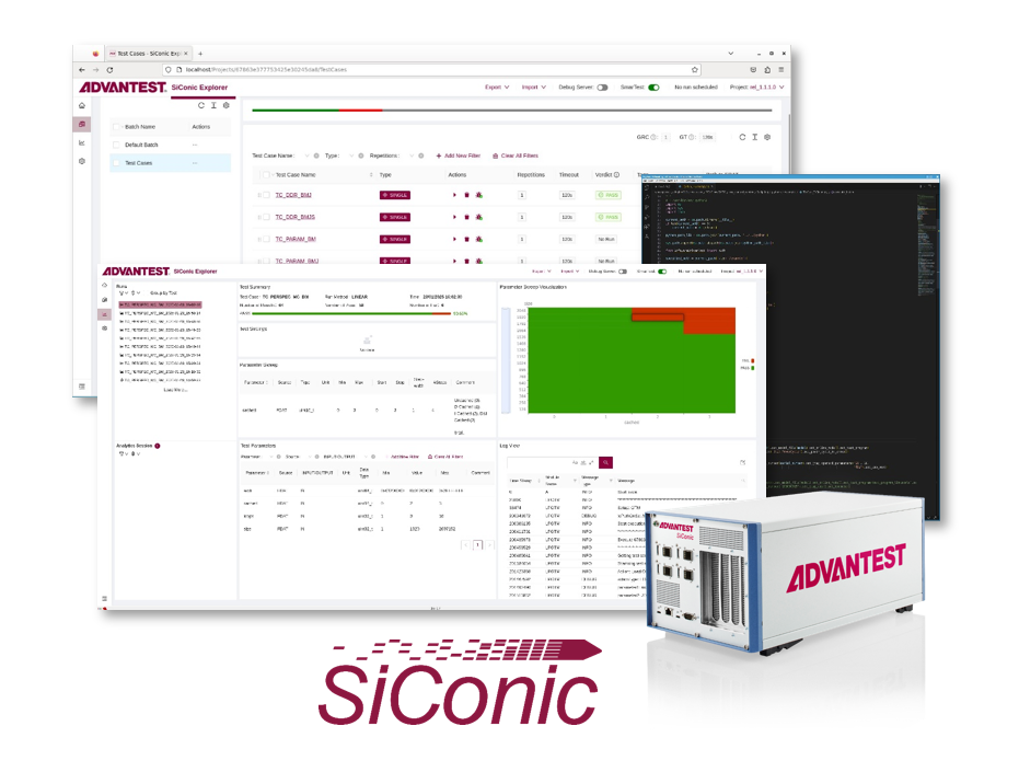
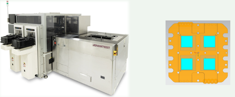
AI Memory: Enabling the Next Era of High-Performance Computing
By Tadashi Oda, Senior Director of Memory and System Engineering, Advantest America
The rapid advancement of artificial intelligence (AI) is driving unprecedented demand for high-performance memory solutions. According to TechInsights, AI-driven applications are fueling a 70% year-over-year growth in high-bandwidth memory (HBM). However, as AI models grow in complexity—from large language models (LLMs) to real-time inference applications—the need for faster, higher-bandwidth, and energy-efficient memory architectures has become critical.
HBM devices consist of multiple stacked DRAM chips. The reduced mounting area and heightened wiring density of the stacked structure improve speed, capacity, and power consumption. Memory-intensive applications, such as high-performance computing (HPC), graphics processing units (GPUs), and AI accelerators, areas once dominated by DDR and GDDR memory, rely on HBM to meet the data throughput requirements of training and inference. At the same time, power-efficient alternatives such as low-power double data rate (LPDDR) are gaining traction in AI servers, where energy consumption is a primary concern. These trends, alongside the increasing integration of AI in mobile and edge applications, are shaping the future of AI memory technologies. However, these advancements bring significant test and validation challenges, requiring innovative solutions to ensure performance, reliability, and cost efficiency.
Market evolution and growth drivers
AI has become the dominant driver of innovation in the semiconductor industry, creating unprecedented demand for memory technologies. The computational complexity of AI models—particularly large language models and generative AI applications—has pushed GPUs and AI accelerators to their limits, requiring memory solutions that can sustain high-speed data access and processing; see Figure 1. HBM has emerged as the preferred solution for AI training workloads, offering multi-die stacking architectures that significantly increase memory bandwidth while minimizing power consumption.
Figure 1. AI data: near-memory compute for energy-efficient systems.
Beyond training, AI inference workloads are expanding into new applications, including mobile devices, automotive systems, and consumer electronics. These deployments require memory solutions optimized for efficiency, low power consumption, and cost-effectiveness. LPDDR, originally designed for mobile applications, is now gaining traction in AI servers due to its ability to deliver high performance with reduced power usage. As AI continues to move from centralized data centers to distributed computing environments, the demand for diverse memory architectures will continue to grow.
Investment in AI infrastructure is accelerating, with hyperscale data centers expanding their AI server capacity to accommodate increasingly complex models. AI workloads require not only high-performance memory but also specialized storage solutions that can handle vast datasets efficiently. The expansion of inference applications beyond data centers is also reshaping memory demand, as AI capabilities are integrated into smartphones, autonomous vehicles, and edge computing devices.
While AI-related markets are seeing rapid growth, traditional memory markets—including automotive, PCs, and mainstream mobile devices—are experiencing soft expansion. This shift reflects the broader industry transition from general-purpose computing to AI-driven architectures. As more AI workloads transition from training to inference, the balance of memory demand will continue to evolve.
AI memory architectures rely on advanced packaging techniques to optimize performance and power efficiency. The adoption of 2.5D / 3D stacking, heterogeneous integration, and silicon interposers enables higher memory densities and faster communication between memory and processors, as shown in Figure 2. These innovations improve AI system performance but introduce new challenges in manufacturing, validation, and test.
Figure 2. A diagram showing a typical HBM DRAM stack.
Ecosystem collaboration is also essential to advancing memory packaging technologies. Memory vendors, semiconductor foundries, and AI chip manufacturers must work closely to ensure seamless integration of next-generation memory architectures. Multi-die stacking and interposer-based designs require sophisticated testing and validation processes to detect defects early and optimize yield. As AI-driven memory solutions become more complex, new test methodologies will be required to ensure reliability and scalability.
The AI memory supply chain is undergoing a significant transformation, with increased vertical integration among semiconductor companies. Leading foundries are expanding their role in memory packaging and testing, consolidating manufacturing processes to improve efficiency. This shift requires closer collaboration between memory suppliers, GPU manufacturers, and semiconductor fabs to optimize design and production workflows.
At the same time, supply chain constraints—particularly in high-performance silicon interposers and through-silicon via (TSV) technologies—are impacting memory production. AI-driven demand for HBM and LPDDR is straining existing manufacturing capacity, making supply chain coordination more critical than ever. Companies must navigate these challenges while maintaining production efficiency and meeting the growing needs of AI applications.
Technology advancements in AI memory
HBM has become the foundation of AI computing, evolving from traditional DDR and GDDR memories to multi-die stacking architectures that deliver extreme bandwidth and low latency. Figure 3 depicts this evolution. The ability to stack multiple memory dies vertically and integrate them with high-speed interconnects allows AI accelerators to process massive datasets more efficiently. However, these advanced designs present unique challenges in manufacturing and test.
Figure 3. Descriptions of commonly used types of memory devices.
As AI workloads expand beyond data centers, power efficiency is becoming a key consideration in memory design. LPDDR, originally developed for mobile devices, is now being adopted in AI servers to reduce power consumption while maintaining high performance. Although LPDDR carries a higher upfront cost than traditional DDR memory, its long-term energy savings make it an attractive option for large-scale AI deployments.
Balancing performance, cost, and power efficiency is a major challenge for AI memory architects. LPDDR must be rigorously tested to ensure it meets the performance demands of AI applications while maintaining the power-saving benefits that make it viable. As AI adoption grows in power-sensitive environments such as mobile and edge computing, LPDDR is expected to play an increasingly important role in AI memory solutions.
AI workloads require specialized storage solutions that can handle the massive data volumes associated with model training and inference. Enterprise AI storage relies on high-speed solid-state drives (SSDs) designed to support AI-driven workloads, enabling fast data retrieval and processing in hyperscale data centers. Meanwhile, edge and on-device AI applications depend on Universal Flash Storage (UFS), a high-speed, low-power interface optimized for flash memory in mobile devices.
Ensuring the performance and reliability of AI storage solutions requires advanced testing methodologies. Both enterprise SSDs and mobile UFS solutions must be validated under AI-specific workloads to ensure they can handle the demands of real-time AI processing. As AI applications continue to diversify, memory and storage technologies will need to evolve accordingly.
Another AI memory function advancement is processing-in-memory (PIM) technology. AI training and inference require significant computational or mathematical resources to operate a combination of matrix multiplications, vector operations, activation functions, or gradient calculations. Figure 4 illustrates the benefits of implementing PIM in conjunction with LPDDR.
The purpose of PIM is to implement processing features inside the memory chip to reduce data movement between the memory and the processor. Because it reduces power consumption and increases performance, PIM is considered particularly effective in the mobile space for enabling a range of AI-powered applications. PIM is one example of how semiconductor memory is a critical component for the AI industry and illustrates how technology continues to evolve to advance future AI capabilities.
Figure 4. Memory in the AI/ML and data era.
Key market and test challenges for HBM
Ensuring the reliability of HBM stacks requires multiple test insertions throughout the production process. Each die within the stack must be validated for performance and integrity before final assembly, as shown in Figure 5. Before stacking, manufacturers perform wafer test that consists of burn-in stress, trimming, failure analysis and repair processes to ensure all memory cells work properly. The logic base die is also tested at wafer-level through SCAN test, IEEE1500 test, and logic test. Additional tests are performed after the DRAM die are stacked on top of the logic base die wafer, including burn-in stress test, DRAM array test, logic die test and high-speed operation test to ensure proper TSV connectivity within the DRAM stack. Advantest has been collaborating with DRAM vendors to develop HBM tests since before volume production began. As a result, the company now supports all test processes essential for the mass production of AI devices.
Thermal management is also a critical consideration, as the increased power density of HBM configurations can lead to overheating and performance degradation. As AI workloads continue to push memory technology forward, new innovations in stacked memory design and thermal control will be essential. Relating to thermal management, the high-power consumption of AI memory solutions is also a concern. Enhanced thermal control solutions, including precision cooling mechanisms, are necessary to address heat dissipation challenges.
Increasing AI memory complexity heightens the challenges associated with the testing and handling of these devices. Ensuring die integrity during stacking and transportation requires the development of specialized die carriers to mitigate physical damage. Advances in automated handling systems improve secure stacking and assembly, reducing manufacturing defects.
The memory supply chain is also evolving, with vendors collaborating more closely with fabs and GPU manufacturers. The shift from siloed production models to integrated development ecosystems aims to overcome supply constraints and streamline production. However, challenges remain, particularly in securing high-performance silicon interposers and TSV technologies, which are essential for advanced memory integration.
Figure 5. Test and assembly process for advanced memory devices.
Advantest’s solutions and market leadership
Advantest is at the forefront of AI memory testing, offering comprehensive solutions that address industry challenges. Various products in the company’s T5000 series, such as the T5833, provide high-speed, high-accuracy testing for HBM configurations, incorporating multi-step validation processes to ensure die integrity. Its modular architecture provides flexibility to scale with evolving test requirements, optimizing cost and efficiency for high-throughput production environments. This means that the platform is prepared for future testing of LPDDR6 devices as well as mobile storage protocols like UFS.
Moving forward in this space, HBM4/E increases power consumption, doubling the DQ pin count in the DDR bus to 2048 DQs. The industry is also considering the development of “custom HBM” to tune specific areas of the AI workload. Advantest is working with industry-leading GPU and ASIC companies and hyperscalers to prepare for custom HBM testing.
Advantest’s proprietary die carriers ensure secure handling, minimizing physical stress on stacked memory dies and preventing defects during high-volume production. The company recognizes the need for handlers that provide superior thermal capabilities to address the growing demand for precision temperature management in AI memory applications.
The latest addition to the T5000 series, the T5801 ultra high-speed memory tester, is engineered to support the latest advancements in high-speed memory technologies —including GDDR7, LPDDR6, and DDR6— critical to meeting the growing demands of AI, HPC, and edge applications. Featuring an innovative front-end unit (FEU) architecture, the system is uniquely equipped to handle the rigorous requirements of next-generation DRAM modules, delivering industry-leading performance of up to 36Gbps PAM3 and 18Gbps NRZ.
The modular and scalable T5851 platform reflects Advantest’s deep collaboration with industry leaders to meet the evolving needs of mobile storage. Designed in close partnership with leading mobile device companies and NAND manufacturers, the system has been supporting multiple generations of PCIe protocols. Its system-level test capabilities enable realistic workloads, ensuring read/write performance, link stability and storage reliability under actual operating conditions. With support for emerging standards like PCIe Gen 6 and UFS M-PHY6.0 using PAM4 signaling, the T5851 showcases Advantest’s commitment to co-developing future-ready solutions for next-generation AI devices.
Conclusion
As AI memory technologies continue to evolve to support increasingly complex workloads, Advantest remains a trusted partner in delivering reliable, scalable, and high-performance memory test solutions. With a vertically integrated strategy, Advantest distinguishes itself as a leader in testers, handlers, and load boards, offering broad support across the memory test ecosystem. Trusted by leading semiconductor manufacturers, Advantest works closely with industry partners to innovate and develop unique solutions that meet their needs.
Moreover, Advantest ensures its platforms are aligned with emerging standards and practical requirements. The T5000 series—including the T5833, T5835, T5503HS2, T5801, and T5851—reflects this commitment, offering modular, high-speed, and flexible solutions for a wide range of memory and storage technologies, from AI-critical HBM to LPDDR, GDDR, DDR, NAND, NOR, and beyond.
Advantest’s continued innovation in areas such as die carriers and thermal management helps address the physical and operational challenges of stacked memory and high-power AI applications. As AI workloads expand across data centers, mobile, and edge environments, the company remains focused on advancing test methodologies that support performance, reliability, and efficiency.
With a forward-looking roadmap and strong industry partnerships, Advantest is well-positioned to support the next generation of AI memory architectures, helping customers navigate complexity and drive innovation in the AI era.