Pages Menu
TwitterRSSFacebook
Categories Menu

Posted in Q&A

Test Challenges Grow for DRAMs and HBM – Q&A with Jin Yokoyama

This article is adapted with permission from a Q&A with Advantest’s Jin Yokoyama, senior director and memory product marketing manager, with Mark LaPedus from Semiecosystem. The original article can be viewed here.

Q. In general, how do we test the latest DRAMs? Isn’t there a test flow involved here? Can you briefly describe the basic test flow for DRAMs and each step?

A. Typically, for DRAM devices, the test flow starts with wafer-level test. At the wafer level, our test systems apply memory test algorithms at varying speeds to test DRAM performance. The DRAM device is then tested again after it is assembled into a package. The final test stage runs tests at operational speed to confirm whether the device processes data correctly and meets end-use requirements.


Q. Over the years, DRAMs have become more complex. What are some of the technology trends that you see with current and future leading-edge DRAMs?

A. We see myriad trends emerging as DRAM technology evolves. DRAM devices are playing a critical role across a variety of applications, including artificial intelligence (AI)/high-performance computing (HPC), data centers, smartphones, AI PCs, and video game consoles.

The growth of AI, specifically, has led to an increase in demand for DRAM devices with higher per-pin speed, higher bandwidth, and low latency. Meanwhile, data centers and AI edge applications require devices to integrate new industry standards for speed and power consumption, including GDDR7, LPDDR6, and HBM4. These devices must also have lower output levels to maintain accuracy and higher operational efficiency to reduce cost.

We also see the trend of miniaturization and the shrinking of bit cells. There is a shift in size to 3,000 devices under test (DUTs) per 300mm wafer, leading to higher density that makes DRAM devices more vulnerable to defects. This means that these devices will likely require more tests and screening to meet demands for quality and reliability. Further densification of tester resources and technology will be necessary to accommodate device miniaturization trends.

Q. What are some of the test challenges with the latest DRAMs?

A. The increasing speed of these devices certainly presents a challenge in the test process. Speed performance requirements for at-speed interface testing on DRAM devices are increasing from 4.5 Gbps to over 10 Gbps, requiring high-performance test equipment to run test algorithms at high operational speeds.

We also need test systems that can test more devices in parallel to maintain lower costs. This requires highly specialized probe card technology that can handle high-speed testing. Massive levels of parallelism will be vital, as the industry trends toward requiring only one touchdown per wafer. Miniaturizing DRAM devices also makes them more susceptible to defects, requiring more thorough testing in the form of burn-in test at the wafer and package levels. Moreover, thermal requirements for DRAM devices continue to rise alongside demands for higher power and bandwidth capacity, and the complexity of integrating DRAM in 2.5D/3D packaging poses its own set of unique test challenges.

In the DRAM market, where high bandwidth and high performance continue to increase, Advantest recently introduced a next-generation ultra-high-speed solution, the T5801. This cutting-edge platform is engineered to support the latest advancements in high-speed memory technologies – including GDDR7, LPDDR6, and DDR6 – critical to meeting the growing demands of AI, HPC, and edge applications.

Q. What are some of the technology trends and challenges that you are seeing with HBM?

A. AI and HPC devices are demanding higher and higher processing speeds to power advanced applications like large-language models (LLMs). HBM consists of multiple DRAM chips stacked vertically. This structure allows for faster and more efficient data transfer with a smaller footprint, which is why HBM plays a key role in data centers. Of course, these HBM devices are incredibly complex and pose various challenges during testing. With multiple DRAM ICs stacked on top of each other, these devices are extremely dense and produce a lot of heat, which poses a risk to the structure of the device. Test systems must be equipped with the proper thermal-management capabilities and refined handler/probe equipment needed to monitor potential hotspots and dissipate heat.

The density of device circuitry and the number of DRAM devices stacked is increasing with each generation of HBM, moving from 8 stacks to 12, 16 and even 24. This has led to longer test times, especially as HBM migrates much faster than traditional memory technology transitions by generation. Higher interface speeds and higher bandwidth of HBM devices also mean high test speed and an increased load on peripheral circuits, requiring high-speed probing technology. Moreover, increases in power supply and current capacity require scalability.

The 2.5D/3D packaged structure of HBM devices also poses significant challenges, requiring thorough testing before the devices are packaged together. More and more manufacturers are looking to utilize die-level test, i.e., testing individual die after the wafer has been diced, to ensure that the DRAM ICs function properly before they are stacked into an HBM device and packaged, increasing overall yield and reliability. “Known-good die” or KGD testing, as it’s sometimes called, helps to prevent manufacturers from assembling packages containing defective die. If even one die in a stack is defective, then the entire package must be disposed of at great cost to the manufacturer.

Q. Are there any test challenges when the industry migrates to HBM4?

A. The greatest challenge we will see is the rising complexity of HBM4 devices. HBM4-based logic wafers are being made at leading-edge logic foundries for use in high-performance data centers to power AI edge applications. This will make the supply chain more complex, and the requirements and manufacturing and testing processes for DRAM manufacturers, foundries, and SoCs will also become more complex as a result. So, more advancements will have to be made in test process optimization in the future to support the next generation of HBM.

Read More

Posted in Q&A

Interview with Oded Olansky, VOICE 2025 Chairperson

Advantest’s VOICE 2025 Developer Conference will take place May 12-14 at the AT&T Conference Center in Austin, Texas. To learn what VOICE 2025 holds in store for attendees, we interviewed this year’s general chairperson, Oded Olansky, WCS RF Products Si Test Architect and WCS Haifa Wireless Test Engineering Manager, Intel.

By GO SEMI & Beyond Staff

Q. With VOICE 2025 taking place in Austin, how will this year’s location impact the event?

A. Austin is significant to the semiconductor industry. Major companies like Tesla, Amazon, AMD, Microsoft, and NXP have a strong presence in the area, with Texas Instruments located nearby in Dallas. This makes Austin a vibrant hub for industry and innovation, which is why we believe it is the perfect location for VOICE 2025. With our venue situated in the bustling heart of the city, we are excited to host VOICE 2025 in Austin and invite our attendees to enjoy the city’s rich culture.

Q. As the VOICE 2025 chair, what do you hope to see, or what do you hope attendees will gain?

A. For me, the VOICE conference has always represented a unique opportunity to explore emerging technologies and innovative testing methodologies, whether through presentations, kiosks, or invaluable networking opportunities with test engineers from diverse companies and countries. I hope that attendees of this year’s conference will experience the same. Personally, I believe that if, upon returning from the conference, I can apply even one new insight or idea successfully in my work, then the conference has been both successful and worthwhile. I encourage the attendees of VOICE 2025 to set a similar goal for themselves.

Q. I heard that there will be an exceptional number of presentations at this year’s event. What presentation topics and industry trends are you most excited about? 

A. Our committee accepted over 100 technical papers this year, with a record line-up of over 130 presenters. These numbers tell us that people are excited about the state of the industry right now and are eager to discuss the latest trends and innovations with their peers. 

I believe we are currently witnessing a transformative revolution in the field of artificial intelligence, particularly in the area of generative AI. This revolution strongly echoes the impact of the Internet revolution, which began around the time I started my career in test engineering. As such, I am particularly eager to see presentations and engage in discussions surrounding this topic, as it promises to reshape the industry in profound ways.

There will also be presentations regarding the new instruments for the V93000 EXA Scale platform that were announced last year, including the DC Scale XHC32 ultra-high-current power supply. Presentations will also feature the new PMUX02 advanced power multiplexer for the V93000, which offers unprecedented capabilities for multi-site testing of power and analog devices, including battery-management systems (BMS), automotive, and power management IC.

Q. What highlights of this year’s event do you recommend attendees not miss?

A. There is plenty to look forward to at VOICE 2025. The conference will kick off on Monday evening with a welcome reception, offering a great opportunity to network with representatives from top semiconductor companies. At the same time, we will host the Technology Kiosk Showcase, featuring exciting displays of cutting-edge innovations that highlight Advantest’s diverse product portfolio.

Tuesday and Wednesday will feature engaging keynotes from semiconductor market analysts and leading professionals. The Partners’ Expo is also open throughout Tuesday and Wednesday, allowing attendees to engage with our technology partners to discuss their latest products and solutions.

Tuesday’s evening event will be hosted at The County Line—a charming lakeside lodge serving classic Texas BBQ and margaritas. The setting provides a relaxed atmosphere that is perfect for mingling with colleagues while enjoying the stunning views of the lake from the venue’s redwood deck. We also have a great lineup of fun Texan-themed activities that everyone can enjoy throughout the evening, including horseshoe tossing and even line dancing lessons. There’s plenty to look forward to, and we invite all attendees to join the fun.

We will wrap up VOICE 2025 on Wednesday afternoon with an awards ceremony honoring the best papers and those receiving honorable mentions. Additionally, we’ll present the Visionary Award, given annually to a customer who has made significant, lasting contributions to VOICE over the years.

Q. Who will be joining us for this year’s keynote addresses?

A. VOICE 2025 will feature three dynamic keynote speakers. 

Our first speaker on Tuesday will be John Yi, a Fellow at AMD. With over 30 years of experience, John currently manages a team of test architects responsible for defining new design-for-test (DFT) methods and test solutions with silicon design and product engineering groups that span a wide spectrum of AMD products. 

Our next two keynotes will be on Wednesday, starting with John Yick, senior director of product and test engineering at Marvell. John leads Marvell’s product and test engineering teams, driving the production of cutting-edge broadband analog devices such as trans-impedance amplifiers and drivers, as well as silicon photonic integrated circuits (PICs). His expertise spans a wide frequency range, from DC to 110 GHz, all the way to light speed.

Roy Meade, TIE executive director of strategic partnerships at the University of Texas, will present our final keynote on Wednesday. Throughout his career, Roy has exhibited exceptional innovation and leadership in the domains of photonics, packaging, and memory technologies. His contributions to these fields are evidenced by over 120 patents granted by the United States Patent and Trademark Office, encompassing photonics, semiconductor manufacturing, and emerging memory technologies.


As a final note, we would like to thank our VOICE 2025 sponsors for making this year’s event possible—in particular, our headline sponsors, ISE Labs, ASE Group and Alliance ATE Consulting Group. The full list of sponsors can be found here.

To learn more about keynotes, papers, and other details related to VOICE 2025, be sure to keep checking the VOICE website. And don’t forget to register here to reserve your spot!

Read More

Posted in Q&A

Interview with Keith Schaub on the Challenges of Testing Today’s Complex Chips

This Q&A is adapted from an article posted to the Semiecosystem blog by Mark LaPedus. It details a conversation with Keith Schaub, vice president of technology and strategy, regarding the test challenges for today’s complex AI chips, gate-all-around transistors, chiplets, and 3D NAND. The original article can be found here.

Q: How has semiconductor test changed over the years?

A: IC test has undergone significant changes over the years, evolving alongside the increasing complexity of semiconductor devices. Initially, testing focused on basic functionality, but as devices grew more intricate, the need for more advanced testing methods emerged. The ATE industry responded by developing new, more capable testers to handle higher pin counts, faster speeds, and greater integration. There was also a shift from purely functional testing to structural testing, which provides deeper insights into the integrity of the chip’s design and manufacturing process. In recent years, system-level testing (SLT) has become increasingly important, enabling verification of complete systems and ensuring interoperability of components. Modern IC tests now include sophisticated techniques such as built-in self-test (BIST) and scan testing, enabling more thorough verification. Additionally, the rise of system-on-chip (SoC) and other advanced technologies has driven the development of testers that can handle multiple functions simultaneously. This IC testing evolution reflects the semiconductor industry’s continual pursuit of higher quality, performance, reliability, and efficiency.

Q: What challenges do you encounter when testing AI devices? 

A: Testing AI chips and accelerators presents several significant challenges due to their complexity and scale. These devices often feature large die sizes, billions of transistors, and dozens to hundreds of cores running at different speeds, depending on workloads. This variability increases the importance of advanced thermal management and control. Ensuring performance and reliability in such dense circuitry requires highly sophisticated ATE capable of handling high-speed interfaces and extreme thermal performance. Hotspots are a critical concern; not only understanding where they occur but being able to predict when they’ll occur during testing is vital for effective thermal control. Comprehensive validation is needed to ensure these chips perform optimally under diverse conditions, particularly in managing power densities and minimizing thermal hotspots. The integration of AI processors with other system components necessitates thorough SLT to verify overall system functionality and interoperability. Additionally, the rapid evolution of AI technology means testing methodologies must continually adapt to keep pace with new architectures and innovations. Overall, these challenges underscore the need for cutting-edge testing solutions to ensure the reliability and performance of AI semiconductor devices.

Q: Tell us more about system-level test. When do you use it in the test flow?

A: SLT is a comprehensive testing methodology used to validate the functionality, performance, and interoperability of semiconductor devices within their intended system environments. Unlike traditional testing methods that focus on individual components, SLT evaluates the entire system, ensuring that all integrated parts work seamlessly together under real-world conditions. 

Over the years, SLT has evolved from being an optional insertion to a mandatory step in the test flow, particularly for complex devices such as AI chips, processors, and SoC solutions, where multiple functionalities and high integration levels are involved. SLT is typically used in the latter stages of the test flow after initial component-level tests have been performed. It follows traditional tests like wafer sort, package test, and burn-in, providing an additional layer of assurance by verifying the complete system’s behavior. For example, in the case of an AI processor, SLT would involve running actual AI workloads and applications to ensure the chip performs correctly within the end-user system. This helps identify any issues related to power management, thermal behavior, and interactions with other system components that might not be detected during earlier test stages.

Q: What new challenges does the transition to gate-all-around (GAA) transistors present?

A: The transition to gate-all-around (GAA) transistors at the 3nm and 2nm logic nodes presents several new challenges for testing. GAA transistors offer improved performance and power efficiency compared to finFETs, but their unique structure and increased density introduce complexities in test processes. One of the primary challenges is ensuring accurate characterization and validation of these advanced transistors, as their electrical properties can be more sensitive to variations in manufacturing processes. Moreover, the increased device density at these nodes requires more sophisticated ATE with higher resolution and precision. Thermal management becomes even more critical due to the higher power densities, necessitating advanced thermal testing techniques to identify and mitigate hotspots. The integration of GAA transistors also demands enhanced DFT and BIST strategies to ensure comprehensive coverage and efficient testing processes. The rapid evolution of these technologies requires continuous updates to test methodologies to keep pace with the latest advancements in GAA transistor design and fabrication. Overall, while GAA transistors at 2nm and beyond promise significant performance benefits, they also necessitate advanced and adaptive testing solutions to address the new challenges they bring.

Q: What are some of the test challenges and ATE solutions for chiplets?

A: Chiplets are generating significant attention in the semiconductor industry due to their potential to enhance performance and flexibility in chip design. However, they introduce several unique test challenges, such as ensuring seamless integration and communication between multiple chiplets within a single package, requiring rigorous testing of interconnects and interfaces. Ensuring known good die (KGD) is critical, as a single defective chiplet can render the entire package unusable, leading to high costs. To address this, shift-left strategies are increasingly important, involving early and comprehensive testing during the design and pre-assembly phases, leveraging AI techniques to enhance test coverage and predict potential failures. The heterogeneous nature of chiplets necessitates highly adaptable ATE capable of handling diverse test requirements. Additionally, SLT is crucial to verify the functionality and interoperability of the combined chiplets under real-world conditions. Thermal management and power delivery are critical, as multiple chiplets within a confined space can lead to hotspots and power distribution issues. Advanced thermal testing techniques and power analysis are required to identify and mitigate these problems.

ATE solutions are evolving to provide higher channel counts, greater flexibility, and improved precision. DFT features, such as BIST and boundary-scan, are increasingly integrated into chiplets to facilitate efficient testing. Overall, while chiplets offer exciting possibilities for innovation, their successful implementation hinges on advanced and flexible ATE solutions, ensuring KGD and employing shift-left strategies enhanced by AI.

Read More

Posted in Q&A

Interview with Doug Lefever, Representative Director and Group CEO

By GO SEMI & Beyond Staff

At the start of the new fiscal year in April, Advantest Corporation officially appointed Doug Lefever as its new Group CEO. Lefever has been with the company for 25 years, serving as Corporate Vice President, Group COO, and President & CEO of Advantest America prior to his new role. We interviewed Lefever to learn more about his plans as CEO.

Q: Could you start by telling us a little bit about your history with Advantest?

A: Advantest has been a major part of my life—and it would not be an overstatement to say that the company has helped to shape who I am as a person. I joined Advantest in 1998—just three years after I graduated from college. Since then, I’ve had the pleasure of watching this company grow into a global leader in ATE manufacturing. I have served in many different capacities in my 25 years with Advantest and have touched most parts of the company in some shape or form, growing long-lasting relationships with key customers and maintaining an in-depth knowledge of our test solutions. I’ve also had the valuable opportunity to participate in key business decisions that have played a part in Advantest’s success, such as the acquisition of Verigy in 2011, which is directly responsible for Advantest’s #1 position in SoC testers. 

Q: What are your plans for steering Advantest through current industry challenges? 

A: Under the leadership of Yoshida-san, we have achieved strong performance in the past few years, greatly increasing our revenues and market capitalization and becoming the world’s number one ATE supplier. To continue this success, we must focus on listening to our customers so that we can meet customers’ needs by supplying them with high-quality, cost-effective test solutions where and when they need them. To this end, we must remain flexible so that we can adjust to market and societal demands.

As semiconductor devices continue to become more complex, our role in solving testing challenges grows. Our customers face challenges in advanced packaging and temperature control. We need to invest more in advanced R&D to further research in test cells and test flows. This will require close collaboration with customers and business partners as we work together to overcome challenges. Our greatest strength is our customers. Our ability to respond and adapt to their needs, especially for mission-critical applications, is the biggest factor in our success. 

Q: What unique traits/characteristics do you believe you bring to the role of CEO?

A: I believe that change and growth come from within, and I think communicating directly with employees and getting to know people within the company is very important. For example, I often host “Coffee Talks” at the offices I visit. These are casual, free-form dialogues where I invite employees to ask questions, discuss market trends, and talk about recent innovations. I like to build trusting relationships with our employees and engaging with them directly allows me to learn more about their perspectives. 

I also see my technical background and long tenure at Advantest as having great value in promoting Advantest’s innovation and building customer relationships based on trust. This powerful combination is important to our continued growth and advancement.

Q: You will be the first American CEO in the company’s history. How do you plan to navigate managing a Japanese company with an American background?

A: Advantest is a global company with over 96% of our sales coming from outside of Japan. As such, I aim to bring a global perspective to the role while preserving Advantest’s roots. Our company was founded in Japan, and its corporate culture is deeply rooted in Japanese customs. I don’t want to change Advantest to fit an outside perspective. I aim to do the opposite: I want to bring Advantest’s unique corporate identity outside of Japan and expand the company’s global reach. I believe this will become even more important to our success and longevity as the semiconductor industry continues to grow around the world.

Q: Lastly, Advantest is celebrating its 70th anniversary this year. Could you say a few words about what this milestone means to you?

A: As I mentioned earlier, I have dedicated my entire career and most of my adult life to working for Advantest. This company is more than just a workplace for me; it is part of who I am. I am immensely proud to lead a company that has achieved such longevity and trust within the industry. We have been able to reach this milestone because we have not only kept up with but anticipated changing market needs. Moving forward, we will remain future-oriented and committed to achieving great things. We will also work wholeheartedly to fulfill our responsibilities to all stakeholders, including our planet. Achieving true sustainability in everything related to our company should be the cornerstone of our success.

I consider this milestone a huge achievement, and I am excited to commemorate it with my colleagues and industry partners in my new position as CEO.

Read More

Posted in Q&A

Interview with Linda Haenel, VOICE 2024 Chairperson

By GO SEMI & Beyond Staff

Advantest’s VOICE 2024 Developer Conference will take place June 3-5 at the Hilton La Jolla Torrey Pines in San Diego, California. To learn what VOICE 2024 holds in store for attendees, we interviewed this year’s general chairperson, Linda Haenel, application consultant, Performance Digital Center of Expertise, Advantest Europe.

Q. With VOICE 2024 taking place in San Diego, how will this year’s location impact the event?

A. San Diego holds great importance for our industry. We anticipate large attendance at this year’s event due to the significant local presence of major semiconductor companies such as Qualcomm, NXP, and Infineon, as well as the location’s relative proximity to Silicon Valley. Also, with the Semiconductor Wafer Test Conference also being held June 3-5 at the Omni La Costa in Carlsbad, we will likely experience some cross-traffic between SWTest and VOICE. We are thrilled to be hosting VOICE at a location that is both accessible and beautiful, with this year’s venue nestled alongside the California coast, offering breathtaking views of the Pacific Ocean.

Q. As the VOICE 2024 chair, what would you hope to see, or what would you hope attendees will gain?

A.  As they do every year, the members of the VOICE committee work hard to offer a memorable event where industry experts come together to share information, learn, collaborate, and network. I want each attendee to come home with something – a new thought, idea, or contact that will inspire them. We’ve built VOICE to be a platform that fosters the exchange of great ideas, leading to the innovations that propel our industry forward, “beyond the technology horizon.” We’ve adopted this theme once again because it is so descriptive – VOICE has always strived to deliver a glimpse beyond that horizon, through test experts’ papers, panels and kiosk presentations, to future advancements.


Q. This year marks Advantest’s 70th anniversary. What does this milestone mean to VOICE?

A.  In many ways, VOICE is emblematic of the relationships Advantest has developed over the past 70 years that have led us to where we are today. Many of the companies participating have worked with Advantest for decades, developing creative products and innovations that pioneered new standards for our industry. We are incredibly grateful to celebrate this milestone with them, and we’re excited to think about what the future, and our 100th anniversary, will bring as we continue to work closely together. 

Q. What are some of the hot trends and topics for 2024?

A.  Our committee accepted more than 100 technical papers this year – a new VOICE record. These papers are distributed over nine technical tracks, and we expect Test Methodologies, High-Performance Digital, and 5G/Millimeter Wave to be featured significantly during the technical sessions.

We are excited to introduce a new Artificial Intelligence (AI) track for VOICE 2024. This track will examine how engineers can benefit from utilizing AI applications in semiconductor production test for data analysis. Papers will also explore how our industry can utilize AI applications in test engineering to streamline test program development. 

There will also be presentations showcasing Advantest’s new Pin Scale Multilevel Serial for the V93000 EXA Scale platform. Released last year, this new product is both the first native and fully integrated HSIO instrument that expands the EXA Scale platform to address signaling requirements for advanced communication interfaces. The card’s multi-level capability enables new signaling schemes emerging in HPC/AI and consumer markets, supporting NRZ and PAM4. 

Q. What highlights of this year’s event do you recommend attendees not miss?

A.  As always, there is much to look forward to. The conference will begin with a welcome reception on Monday evening that will offer a valuable opportunity to network with representatives from leading semiconductor companies. Concurrent with the reception, we will host the Technology Kiosk Showcase, which will include inspiring displays of the latest innovations that leverage Advantest’s broad product portfolio.

Tuesday and Wednesday will feature engaging keynotes from semiconductor market analysts and leading professionals. The Partners’ Expo is also open throughout Tuesday and Wednesday, allowing attendees to engage with our technology partners to discuss their latest products and solutions. 

I am especially excited for Tuesday’s evening event that will take us to the Birch Aquarium, where attendees will enjoy a lovely evening dinner alongside exhibits featuring tropical fish, Leopard Sharks, giant kelp forests, and Little Blue Penguins. The Birch Aquarium is associated with the University of California San Diego’s Scripps Institution of Oceanography and, much like Advantest, maintains a strong commitment to sustainability and local conservation efforts. We look forward to learning more about how we can preserve our oceans and the unique wildlife that lives beneath the surface. 

We will close VOICE 2024 on Wednesday afternoon with an award ceremony celebrating the best papers and honorable mentions. We will also give out the Visionary Award, presented annually to a customer who has made significant, sustained contributions to VOICE over a long period.

Q.  Who will be joining us for this year’s highly anticipated keynote addresses?

A.  I am pleased to announce that VOICE 2024 will feature three dynamic keynote speakers.

Our first speaker, on Tuesday, will be Craig Nishizaki, vice president of the Test Solutions Group at NVIDIA, which is responsible for providing manufacturing hardware and software test solutions for all NVIDIA’s products, from chips to boards to servers. 

Our second Tuesday keynote will be delivered by Marcelo Ackermann, professor, XUV Optics Group at the University of Twente (Netherlands), and chair of the Industry Focus Group – X-ray and EUV (XUV) optics at the university’s MESA+ institute. As a professor, he focuses on the development of next-generation reflective, refractive and transparent X-ray and EUV optics in collaboration with industry partners like Zeiss, ASML, and Malvern Panalytical. 

Wednesday’s keynote will be presented by Andrea Lati, director of market research at TechInsights. For more than two decades, Andrea has managed and developed forecasting models as well as performed market analysis and research on electronics, semiconductor, and equipment markets for TechInsights.

As a final note, we would like to thank our VOICE 2024 sponsors for making this year’s event possible—in particular, our headline sponsors, ISE Labs, ASE Group and Alliance ATE Consulting Group. The full list of sponsors can be found here.

To learn more about keynotes, papers, and other details related to VOICE 2024, be sure to keep checking the VOICE website. And don’t forget to register here to reserve your spot!

Read More

Posted in Q&A

Test Needs and Solutions for High-End SoCs

Q&A Interview with Ralf Stoffels

By GO SEMI & BEYOND staff

High-performance computing (HPC) is a major driver for the SoC test market, in which Advantest holds a dominant share. Sustaining and extending this leadership requires capitalizing on the company’s already strong portfolio by pursuing new strategies. Our staff spoke with Ralf Stoffels, Advantest Executive Officer and V93000 Division Manager, who expanded on key points from a presentation given to Advantest investors in December 2022.

Q. Let’s start with the HPC market. What are some reasons it is such a driving force?

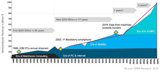
A. The semiconductor industry is widely projected to become a US$1 trillion market by 2030, with three segments representing 70% of this growth: automotive, wireless communications, and computing and data storage. If you look at the evolution of HPC, each new era has emerged more quickly than the last, and we are now at the point where the demand for processing high volumes of data has propelled us into the age of exascale computing (Figure 1). 


Figure 1. Each successive era of computing is evolving orders of magnitude more quickly than the one before, with HPC and AI driving the semiconductor industry toward the $1T mark by 2030.

Q.What are some of the specific HPC trends, and why are they pushing SoC test forward?

A. The technical trends for HPC illustrate the growing level of complexity in these applications. Key trends include: the rise of chiplets, which we’re seeing everywhere; new Arm server CPUs; larger packages for smaller nodes, which are being ramped by computing rather than mobile devices; 3D package constructs, from micro bumps to hybrid bonding; heightened power and thermal demands created by power supplies; and massive communication challenges created by very large, high-speed data networks.

Data centers, one of the primary applications for HPC chips, are essential for training and operating AI models, which are being employed for everything from autonomous driving to advanced chatbot assistants. In turn, this requires access to the tens of thousands of graphical processing units (GPUs) needed to analyze high volumes of data in real time.

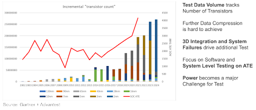
All of these developments together create massive data requirements that result in new test demands to accommodate this 100x rise in complexity, which is pushing the ATE market toward US$10 billion by the end of the decade, as shown in Figure 2.


Figure 2. Fast-growing device complexity is driving the market size for ATE. These indicators point to the total available market reaching US$10 billion by 2030.

Q. HPC processors have a longer product development cycle than those for, say, smartphones. At what point in this process does test become critical?

A. During the early phases of product development, semiconductor manufacturers are focused on improving productivity while optimizing techniques essential to functionality. The need for test is particularly high during these early stages. HPC devices are no different in this respect. There are many test needs associated with ramping new nodes, and next-generation devices are always in development. While test is most critical during early development to achieve desired functionality and eliminate bugs, test needs will be consistently distributed across the lifetime of new and emerging devices.

Q. How has the V93000 contributed to Advantest securing its strong market position in SoC?

A. We’re addressing these complex demands with the latest offshoot of our flagship V93000 platform, the V93000 EXA Scale. Establishing V93000 as a scalable platform has allowed us to continually expand its range and functionality to accommodate testing devices for a wide range of applications. This flexibility is a core element of the V93000’s long-term success. We were also the first ATE company to establish long-term compatibility with a single test platform – this is crucial for customers migrating to the next generation of test capabilities. In addition, through our market leadership and customer relationships, we understand what lies ahead for the industry so that our R&D efforts continue to stay on top of HPC requirements.

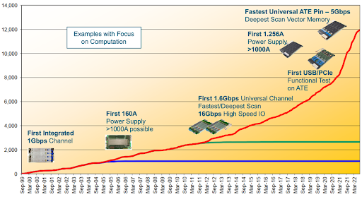
Figure 3. Advantest has continually developed industry-first HPC-level capabilities for the V93000 SoC test platform.

Figure 3 illustrates the evolution of our leadership in HPC innovations, highlighting some of our computationally focused developments. One of the more recent of these developments is the XPS256 device power supply (DPS), which scales from milliamps to more than 1000 amps, covering all power requirements in a single DPS card. We are seeing a number of existing V93000 customers make the transition to EXA Scale for the system’s inherent capabilities as well as options such as the XPS256 and the Pin Scale 5000. When configured with these cards, the EXA Scale system is well equipped to meet exascale computing requirements for mobile, AI, HPC and other advanced devices.

Q. What else should readers know about HPC test requirements and how Advantest is addressing them?

A. Efforts to continue extending Moore’s Law rest on 3D integration – chiplets, stacked packages, FinFETs, etc. This technology is vital to the future of the industry, and it also generates new and different failure types that we have not seen before, necessitating new test approaches and faster testers. EXA Scale is the only tester that can reach 5Gbps on every pin and also has the deepest ATE memories, allowing it to deal with this advanced complexity. In addition, the XPS256 is fully integrated with the EXA Scale system and digitally controlled, so different channels can all be connected by a digital bus, so they can all be kept synchronized and completely controlled by the computational paths inside the system, with no analog factors. This has never been done before, and it allows us to be faster and much more precise in terms of controlling the voltage as well as protecting the device or the probe card. If something goes wrong, we can switch off immediately.

In addition, customers can execute software and interact with their systems via our Link Scale family of digital channel cards for the V93000 platform, which enables software-based functional testing and USB/PCI Express (PCIe) scan testing of advanced semiconductors. The card essentially behaves like your computer, communicating with the device under test through a standard high-speed serial interface to enable very fast transfer of functional and scan test content. Because the device can be interacted with on the wafer the way they’ll be used later on when they’re singulated and packaged, the user can increase test coverage and throughput simultaneously as well as realize faster time to market. 

As new HPC computing developments arise, Advantest is well-positioned to address concurrent test needs through our V93000 platform and continually expanding portfolio of best-in-class cards and peripherals.

Read More