Pages Menu
TwitterRSSFacebook
Categories Menu

Posted in Top Stories

Adaptable, Modular Platforms Are Key to Future-Focused Test

By GO SEMI & BEYOND Staff

The electronics industry evolves continually, introducing potentially disruptive technologies and driving new applications at a pace that requires companies to respond quickly and nimbly. Being able to recognize trends early on and provide solutions that can adapt to meet emerging demands is key to remaining competitive.

This is especially true of suppliers to the semiconductor ecosystem, including test and measurement solution providers, who must be able to meet the increasingly stringent testing requirements associated with devices developed for everything from smartphones and displays to AI and automotive applications.

A dominant trend is the demand for smart portable devices such as smartphones and tablets to deliver processing performance without significantly compromising battery life. A long battery-charging interval is a huge differentiator that can make or break even the most promising products and technologies. Simply put, people demand long battery life, but still crave faster, smaller, more feature-packed devices with power-hungry connectivity technologies like 5G.

However, solving one problem often produces another. This axiom applies to developing more sophisticated devices, where testing, especially system-on-chip (SoC) testing, has come up against such daunting challenges as higher voltages, data encryption, low-leakage battery-powered designs, more complex chips, and rapid development cycles. Yet test technology providers need to continue to meet the demand for low-cost solutions in high-volume manufacturing environments. Today, the testing space is defined by a broad range of different applications, requiring a similarly large variety of test methodologies. By looking ahead, companies can position themselves early on to benefit over the course of a product’s lifecycle.

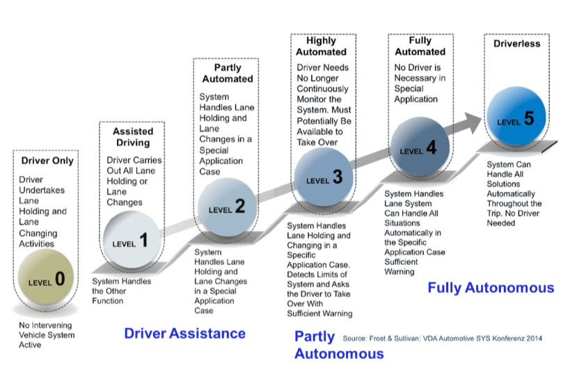
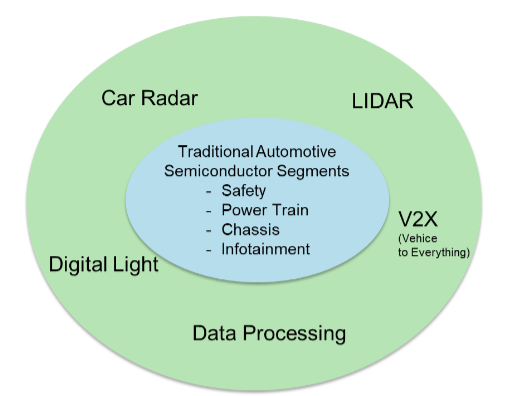
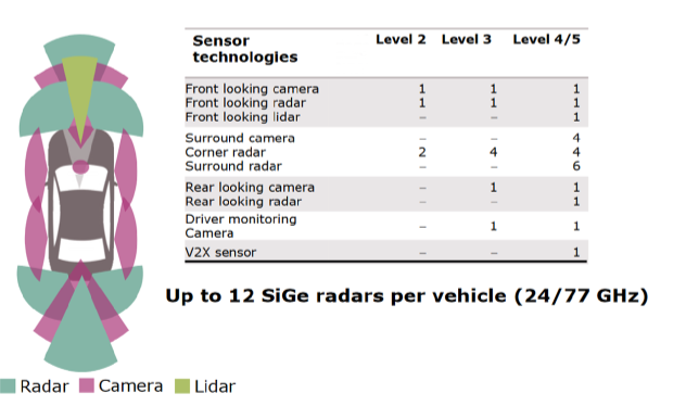
Autonomous cars and e-mobility are leading trends that are under continuous development. These applications have evolved rapidly over the past few years, with the number of electronic components in today’s vehicles having rocketed into the near-triple digits. From infotainment (car navigation, center console control) to autonomous driving (image sensors, AI) to vehicle control (driving assistance, tire pressure monitoring, engine control), this market offers phenomenal potential, both current and future. The more innovations that are developed, the more markets created and the greater the demand. Ensuring automotive-grade, zero-defect quality is essential to guaranteeing safety, reliability, and market success.

Enabling high-quality testing

Advantest has a wide portfolio of solutions with the flexibility and capabilities essential for expanding into sectors where innovation is on the rise. These solutions are all designed to contribute to improving test quality and flexibility while lowering test costs.

The V93000 system is configurable to match device needs, providing DC, digital, analog and RF capabilities on one tester platform. As testing needs change and develop over time, the platform can adapt with the addition of new modules to expand functionality. The RF solution, for example, can accommodate a wide range of devices with varying levels of complexity (such as mobile phones, navigation systems, Wi-FI- and Bluetooth-enabled devices, and IoT systems) – testing up to 32 devices or RF ports in parallel.

Complementing the platform with the power analog FVI16 card enables flexible and transparent high-quality power testing (see Figure 1). The card, which is mainly used for automotive, industrial and consumer mobile charging applications, utilizes shorter test pulses, which prevents heating up the tested device and saves test time, and features a digital feedback loop design for accurate and reliable measurements. It also houses test processor technology with 16 units per card, enabling customers to run tests in parallel, time synchronized and with high throughput.

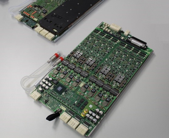
Figure 1: The V93000- FVI16 floating power VI source for testing power is used primarily in the automotive, industrial, and e-mobility markets. (Source: Charlene Perrin)

The Wave Scale RF, MX, and MX HR channel cards are used on the same platform for multi-site and in-site testing of RF and mixed-signal devices. The cards, which each have different capabilities, bandwidths and application targets, were specifically developed to be adaptable to future device test demands.

The T2000 test platform, with air and liquid dual capability, is also available for many different applications, including IoT/module test solutions, automotive and power-management IC (PMIC) solutions (Figure 2). This single test platform can cover all segments, including mobile charging technologies, automotive applications-specific standard products (ASSPs), and battery monitoring. It features high parallelism and multi-site test technology for measuring devices under test (DUTs). The platforms benefits, in addition to reducing test costs and time to market, include providing consistent quality and traceability.

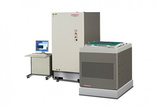
Figure 2: The flexible T2000 test platform performs high-volume, parallel testing of a wide range of SoC devices. (Source: Advantest)

Primarily focused on the automotive and consumer markets, Advantest’s SoC pick-and-place handling systems handle fine-pitch devices while applying precise temperatures. The M4841 system features individual thermal accuracy with high reliability, contact force and throughput. It can operate across a wide temperature range, with very low jam rates. The M4872 has active thermal control with a vision alignment option and fast temperature boost. It also has high contact accuracy and high-power dissipation, to help optimize yield. This system provides failure detection for applications that demand the highest quality.

As technologies evolve into more demanding and complex systems with higher performance capabilities, the future of semiconductor testers will require ongoing development. Advantest is one company that intends to grow along with these and other future innovations, adhering to its strategy of keeping test costs low while delivering high-quality, reliable testing solutions.

Read More

Posted in Top Stories

Parallelism Reduces Cost of Test for IoT, 4G, 5G, and Beyond

By Dieter Ohnesorge, Product Manager for RF Solutions

Introduction

The proliferation of the Internet of Things and the move from 4G to 5G is bringing about pressing test problems. The challenges will increase as billions of IoT devices incorporate GPS, Bluetooth, WLAN, NB-IoT, LTE-A, LTE-M, and other connectivity technologies and as smartphones begin connecting with 5G networks. Applications extend from M2M communications to fixed and mobile wireless access in smart cities. Venues for deployment will extend from factories and vehicles to stadiums and airports.

Transceiver chips for such applications include an increasing number of bands and RF ports carrying high-quality signals. The result can be longer test times leading to increasing cost of test.

Parallel test flow

Many transceivers have architectures that support testing paths and bands in parallel to reduce the cost of test with test techniques that are closer to mission mode, with the test mimicking real-life operation. For example, while you are making a phone call in your car, your smartphone is connected to a cell tower but also to your hands-free Bluetooth connection. You are also likely navigating by GPS and may use a WLAN connection to download a video for your kids to watch. All these functions are taking place in parallel, and an effective production-test strategy should come as close as possible to applying these mission-mode parallel operations.

Traditional “serial” test-flow techniques, based on a fanout RF architecture with shared stimulus and measurement resources, cannot cost-effectively test complex devices. For an LTE-A transceiver with carrier aggregation, a serial test approach would need to test the various uplink and downlink channels sequentially in a series of RF stimulus and baseband measurement operations followed by baseband stimulus and RF measurement operations—leading to long test times.

An alternative is the parallel test flow, enabled by an architecture incorporating independent RF subsystems with truly parallel stimulus and measurement ports. A parallel test flow can speed the test of multiple ports in a single device and can also support multisite test.

WSRF LTE-A/RF combo device test example

The parallel test technique is enabled by instruments such as the V93000 Wave Scale RF (WSRF) card, which offers test-processor-based synchronization and parallel mission-mode test capability. WSRF can simultaneously test multiple transceiver channels in parallel, thereby improving multisite efficiency (MSE) and significantly reducing test time.

The WSRF includes four independent RF subsystems on each card, with 32 truly parallel stimulus and measurement RF ports per card. Each RF subsystem includes an embedded arbitrary waveform generator and digitizer. The WSRF supports 16x multisite test with native ATE resources and includes embedded RF calibration standards.

For less demanding IoT applications, the WSRF scales down to one RF subsystem for use in an A-Class V93000 system. The WSRF can scale down for IoT, enabling it to perform quad-site testing based on one-fourth of a card using just one RF subsystem. At the other end of the spectrum, you may need four WSRF cards to cover the different needs for both sub-6-GHz and mmWave frequencies.

A concept study involving an LTE-A RF transceiver/RF combo device with 802.11ac support and a 3G/4G front-end module showed that the WSRF resulted in test-time improvements of up to 50% as compared with the PSRF, the predecessor to the WSRF.

Figure 1 (not to scale) depicts receive-channel, transmit-channel, and other tests performed serially (top) and the same tests using a mission-mode parallel technique (bottom). Parallel mission-mode test coupled with test-processor-based synchronization can provide a 40% to 60% test-time reduction. Figure 2 provides specific test-time-reduction values for testing parameters such as gain and EVM in single- and quad-site formats, showing MSE and test-time improvement. The results are based on similar setups and sample rates, with the patterns used being the same.

Figure 1. A serial test technique (top) cannot cost-effectively test complex devices, whereas a parallel mission-mode test (bottom) can result in a 50% test-time reduction.


Figure 2. This overview shows multisite efficiencies (MSE) and test-time improvements for parallel vs. serial receiver tests.


Testing 802.11ax

Test of 802.11ax devices offers another example of the benefits of parallel test flow. The successor to 802.11ac, 802.11ax offers an expected fourfold increase in user throughput. Designed to improve overall spectral efficiency in dense deployment scenarios, 802.11ax incorporates multiuser MIMO on the downlink and uplink. It operates in both the 2.4-GHz and 5-GHz ISM bands.

These characteristics impose significant ATE challenges. Multiuser MIMO places more demands on RF/analog resources, resulting in longer test times. ATE RF and baseband instruments (AWGs and digitizers) must accommodate the standard’s 160-MHz bandwidth, and the 1024 QAM modulation scheme demands improved phase noise and linearity.

An eight-site test of an 802.11ax transceiver operating in the 5-GHz band with 4×4 MIMO demonstrates how Wave Scale technology and SmarTest 8 software can test over 4,000 test items, including transmitter, receiver, power-detection, DC, and functional test parameters. The Wave Scale technology includes the Wave Scale RF plus the Wave Scale MX, which includes 16 AWGs, 16 digitizers, 64 PMUs, a hardware sequencer, a real-time signal-processing unit, and a large waveform memory.

Complementing the Wave Scale cards, SmarTest 8 protocol-aware software works directly with user-defined register files and generates a protocol-aware sequence using device-setup APIs with no additional conversion required. The software supports the easy-to-implement flexibleA-Class parallel programming required for concurrent testing. An automated bursting capability works with any type of test, including DC, RF, and digital, and runs as fast as tests based on flat patterns, eliminating the need for manual test-time-reduction efforts, thereby providing an early throughput advantage.

In the 802.11ax example, the Wave Scale instruments powered by SmarTest 8 can test four transmitters concurrently in about 23 ms, vs. 80 ms for a serial-measurement approach, resulting in a test-time reduction of about 70%.

Moving to 5G

5G chips are appearing on the market and can be expected to find their way into 5G handsets and infrastructure equipment in the coming months as 5G deployments roll out. Such devices will increasingly need to rely on parallel test flows to handle the complexities of 5G while continuing to provide backwards compatibility with 3G and 4G technologies, and as they continue to support WLAN, GPS, ZigBee, Bluetooth, and various IoT connectivity applications.

With respect to 5G, new smartphones and other devices will achieve high peak speeds, and 5G will rely heavily on eMBB (enhanced mobile broadband). eMBB will provide not only improved data rates but also broadband everywhere, including in vehicles extending to high-speed trains. Coupled with carrier aggregation, eMBB provides a further example of the benefit for having a parallel test flow that goes hand in hand with test-time reduction and lower COT.

The Wave Scale cards, available now, stand ready to help customers keep pace with the parallel test demands of current and next-generation semiconductor devices.

Read More

Posted in Top Stories

Pro Sports: A New Frontier for Prosthetics

Judy Davies, Vice President of Global Marketing Communications, Advantest

Professional sports demand a great deal of the athletes who pursue them, and many of these players willingly give 110%—a commitment that takes on new significance when a physical disability is involved. The National Football League (NFL), for example, has boasted a number of players who have excelled in this physically demanding sport despite missing body parts.

Legendary San Francisco 49er cornerback and free safety Ronnie Lott, who was elected into the Pro Football Hall of Fame in 2000, mangled his pinkie finger during the 1985-86 NFL season. His competitive fervor was such that he opted for amputation of the damaged fingertip rather than surgery and rehabilitation that would cause him to miss multiple games.

Prior to the era of Lott, Montana, et. al, place kicker Tom Dempsey utilized a custom-built football cleat with a flattened front surface to accommodate a birth defect: the lack of toes on his right foot. Dempsey enjoyed a 10-year career in the NFL, and during the 1970-71 season, he kicked a 63-yard field goal while playing for the New Orleans Saints—a record that remained unbroken until December 2013.

This year, the Seattle Seahawks selected, as one of their draft picks, defensive player Shaquem Griffin out of the University of Central Florida. Griffin has no left hand, having been born with a congenital condition called amniotic band syndrome that necessitated amputation of his underdeveloped left hand at the age of four. However, Griffin’s performance in college, particularly the Senior Bowl in January, greatly impressed pro scouts, and at the NFL Combine event, he bench-pressed 225 pounds 20 times, using a prosthetic hand to grasp the bar. It’s not yet clear whether the NFL will allow Griffin to wear an artificial hand during games—does such special equipment give a player an unfair advantage, or does it simply help level the playing field?

One thing that isn’t in question: prosthetics technology continues to grow in sophistication. Advances in medical knowledge and kinesiology, together with smaller, more efficient microelectronics and longer battery life, are producing such remarkable devices as prosthetic fingers that enable the dexterity and control a wearer needs to perform everyday tasks most of us take for granted.

Dr. Hugh Herr, director of the biomechatronics group at the Massachusetts Institute of Technology’s Media Lab, is a leading pioneer in engineering bionic limbs A double amputee himself, Dr. Herr has designed high-tech prosthetics, such as his computerized BiOM ankle, that restore users’ ability to pursue such activities as running and swimming. Dr. Herr’s focus is on improving the human-machine interface of prosthetics to reduce users’ pain and frustration.

The ultimate goal is to apply advanced semiconductor technology – including sensors, computers and MEMS – to link artificial limbs with the human nervous system. Dr. Herr will share further details regarding his research and its applications when he delivers the keynote address next May at Advantest’s annual VOICE Developer Conference.

Of course, to go along with the nervous system, as the old song says, “You gotta have heart.” Consider the words of Tom Dempsey, whose reported response to those complaining his custom cleat gave him a competitive advantage was, “Unfair, eh? How about you try kicking a 63-yard field goal to win it with two seconds left and you’re wearing a square shoe – oh yeah, and no toes either.” Talent, technology… and heart. Sounds like a winning combination.

Judy Davies, VP Global Marketing Communications


Read More

Posted in Top Stories

PCIe Gen 4 Is Coming – the SLT Solution Is Here

By Colin Ritchie, Vice President, System Level Test Business, Advantest

The high-tech industry is currently in the midst of what has been widely cited by industry experts and executives as a memory super-cycle. Memory manufacturers, in response to sustained high demand for memory devices – including from the solid-state drive (SSD) market – are adding capacity to ensure their ability to meet this explosive demand.

The test requirements for SSDs comprise a wide range of variables that span many different engineering disciplines, as shown in Figure 1. One of the most challenging is the variety of protocols implemented, which vary widely in functionality and performance. Having noted this, it’s clear that the industry is moving toward newer, faster data-transfer protocols.

Figure 1. SSD test requirements include a wide range of variables.

SSD makers have traditionally utilized Serial ATA (SATA) or Serial Attached SCSI (SAS) – both of which, while still in use, are showing signs of age. However, the more compact and easily implemented PCI Express (PCIe) protocol has become highly popular, both in standalone mode and as a transport mechanism for the Non-Volatile Memory Express (NVMe) protocol (which is optimized for NAND flash next-generation NVM technologies).

While the third generation of PCIe (Gen 3) has met with notable success, the industry has been waiting for Gen 4, as it delivers capabilities previously unattainable with other SSD protocols. The new PCIe Gen 4 standardized data transfer bus will double the per-lane data transfer rate of the prior Gen3 revision from 8.0 gigatransfers per second (GT/s) to 16.0 GT/s. As a result, data transfer rates of up to 2GB/s (gigabytes/second) can be achieved with just one PCIe Gen 4 interconnection, and up to 16GB/s with an 8-slot PCIe Gen 4 interconnection for graphics cards and high-end SSDs.

The greatest beneficiary of this new implementation of PCIe will be the burgeoning Big Data arena. With the advent of the IoT and “smart everything,” a host of applications are churning out data in massive volumes. With its speed and capacity, PCIe Gen 4 will dramatically boost server throughput. At the same time, it will also place even greater demands on system-level testing (SLT), which has evolved rapidly to meet growing industry requirements for protocol testing at the system level. In the highly competitive SSD market, a test system that supports multiple protocols can eliminate the need for retooling and help speed transitions between product generations.

Another industry first for system-level test

Advantest’s proven platform strategy is ideally suited to system-level test. Both standard and custom solutions can be economically configured with the implementation of modular components developed for the platform. Its modularity and adaptability also are essential for optimizing manufacturers’ factory-floor configurations to accommodate new product generations – changes can be made quickly and efficiently with a minimum of disruption to the manufacturing process.

The flexible MPT3000 SLT platform was designed to meet customers’ testing needs for both enterprise and client SSDs. Already used by leading manufacturers of PCIe Gen 3, SATA and SAS SSDs, the MPT3000 portfolio has again expanded to accommodate the newest generation of PCIe.

On August 1, Advantest announced its latest industry breakthrough: the first fully integrated test solution for developing, debugging and mass producing PCIe Gen 4 SSDs on the MPT3000. The all-inclusive test solution enables SSD manufacturers to accelerate their newest products’ time to market.

The newly expanded MPT3000 platform is available in three configurations that enable it to cover all test insertions for PCIe Gen 4 devices (Figure 2), without waiting for third-party PCIe Gen 4 infrastructure to be commercially available:

  • MPT3000ES for engineering applications and program development
  • MPT3000ENV for reliability demonstration testing (RDT) and quality assurance (QA)
  • MPT3000HVM for high capacity and throughput in high-volume manufacturing.

Figure 2. The MPT3000 platform can be implemented at every stage of SSD test.

The holistic MPT3000 platform streamlines the transition to PCIe Gen 4 by offering users a test flow that spans design to manufacturing and uses the same tester architecture and software as the proven PCIe Gen 3 offering – giving SSD manufacturers access to the fastest, lowest-risk path to market. Its tester-per-DUT [device under test] architecture and hardware acceleration make the MPT3000 a single-system solution for virtually all engineering, volume production and built-in self-test (BIST) applications.

The newest evolution of PCIe motherboards is expected to begin hitting the market within the next six to 12 months. Developers integrating PCIe into their products need a reliable test solution today to ensure they are able to hit this market window. They need look no further than the MPT3000 PCIe Gen 4 solution from Advantest – available now and already shipping to customers.

Read More

Posted in Top Stories

AI Today – We’ve Come a Long Way

Judy Davies, Vice President of Global Marketing Communications, Advantest

Artificial intelligence (AI) has made amazing technological leaps since what some consider its first implementation: the first programmable digital computer, invented in Germany by Konrad Zuse in 1941. Since then, of course, AI has made amazing technological leaps, while at the same time incurring misconceptions on the part of many regarding its potential uses. Let’s take a look at the current state of AI, and how it’s being enabled by continued evolution of semiconductor technology.

Today’s AI systems comprise advanced software, hardware and algorithms, performing tasks that normally require human intelligence, such as independent learning and problem solving. AI-powered devices can crunch huge amounts of information in a short period of time. The availability of high-speed, low-latency mobile data allows users to access information quickly without a large power requirement, enabling real-time content streaming while making possible a growing range of applications, from augmented and virtual reality (AR/VR), to cloud computing, to “smart everything.”

Cognitive engines are being used by government agencies from municipal police departments to the CIA to sift through and perform intricate analyses of myriad information collected on a daily basis – ranging from fingerprints to images captured on police body-cams. Similarly, California firefighting efforts have benefited from the use of drones to gather on-site information in the midst of raging wildfires, relaying the location of hot spots and overall fire movement. This is particularly valuable when a fire is burning in an area of rough terrain, helping agencies map out the best plan of attack.

But AI is also being used on a more personal level, in human/machine interfaces. These range from ATMs and smartphone GPS, to home-automation devices such as Amazon Echo or Google Home, to our increasingly interactive vehicles. According to market research firm IC Insights, automotive electronics will be the fastest growing IC market segment through 2021. Companies ranging from Porsche to Dyson (best known for its high-end vacuum cleaners and personal electronics) are working to apply this processing power for all-electric and, soon, fully autonomous, self-driving vehicles.

At the heart of a host of these human/machine applications is the ongoing march of semiconductor technology progress, enabling new functionality for new markets. Sensor technology is critical to the development of self-driving cars. A major challenge is equipping vehicles to determine when a turn can safely be made if pedestrians are present. Driverless cars can be made to recognize road signs and proximity of other vehicles, but people entering crosswalks create a unique challenge – the car may sit there indefinitely, waiting until no movement at all can be detected. By viewing autonomous cars as essentially mobile sensors and part the connected “Internet of Everything,” the chip industry can speed its efforts to develop solutions that overcome these hurdles while also enabling new business models.

Illustrating its diversity, AI also has applications in medical markets – for example, creating opportunities for those missing limbs to experience improved mobility. Enabled by smaller, more efficient microelectronics and longer battery life, AI can be combined with advances in medical knowledge and kinesiology to achieve next-generation developments in prosthetics.

Companies such as HDT Global, which partners with DARPA, and Touch Bionics, maker of the i-limb prosthetic hand, are making the most of improvements in microprocessors, software and battery technology to usher in a new era in bionics. Using semiconductor technology, researchers at Brown University implanted a sensor in the brain of a 58-year-old quadriplegic woman. Electrical signals from neurons in her motor cortex were able to command a computer-controlled prosthetic arm to grasp a bottle with the woman’s right hand and bring it to her mouth. A number of further advances in brain-controlled prosthetics are on the horizon, based on presentations given last fall at Neuroscience 2017, the annual meeting organized by the Society for Neuroscience.

Another use of AI revolves around intelligent harvesting of ambient energy from a wide range of common external sources, including photons, geothermal heat and kinetic energy, and harnessing it to improve our human experience through mobile and wireless electronics. An example, demonstrated through technology incubator Silicon Catalyst, harvests body heat to power smart watches and other devices. It does this by leveraging the difference between body temperature and the surrounding air; the larger the temperature disparity, the more energy is available. If the power can be channeled in sufficient quantity to drive all the functions on a smart watch, the wearer could theoretically generate electrical power on the move, anywhere he or she goes.

In concert with all of these developments, advances in test solutions and methodologies are helping to reduce the prices of new electronic devices and ensure their availability in sufficient volumes for mass markets. This is critical at a time when people of all kinds are benefiting from their close connections with technology.

Certainly, securing our private lives, our finances and our communication platforms from identity theft has become a key concern. Even so, the growth in human/machine interactions is highly promising. Our abilities to enjoy active lifestyles, drive vehicles and even keep our communities safe all can be enhanced by the use of electronic devices available today. Emerging semiconductor technologies can take us even further.

Judy Davies, VP Global Marketing Communications

Read More

Posted in Top Stories

ADAS Extends Traditional Automotive Technologies for Autonomous Vehicles

By Toni Dirscherl, Product Manager, Power and Analog Solutions, Advantest Europe

Autonomous cars are one of the most topical, intensely discussed trends in the world today, and will likely continue to be so for the foreseeable future. The reality is that there are degrees of autonomy; if you drive a car manufactured within the last three to five years, you are already using some of this technology. Typically referred to as “passive” autonomous driving, this includes sensors that issue a warning beep when you’re backing up, changing lanes, or come too close to the vehicle ahead.

While fully driverless cars are still farther out on the horizon, we are into the next phase of integrating automated driver-assistance systems (ADAS) into vehicles – i.e., limited driver substitution. This ongoing effort is overlapping the growing focus on making cars with complete autonomous capability available. This article will look at some of the specifics regarding the different levels of ADAS capability, the semiconductor technologies they entail, and the test capabilities that will be required.

From driver-only to driverless

As the illustration in Figure 1 shows, there are several degrees of autonomy that can be designed into vehicle systems. Plenty of cars at driver-only Level 0 are still on the road, and will be for some time, given modern cars’ average age and length of ownership.

Vehicles with Level 1 and 2 features are widely available, and some capabilities that fall under the Level 3 umbrella are becoming available in limited fashion. Levels 4 and 5, of course, are still in the future, but to bring them to fruition will require having regulations in place needed to ensure their safety, which may delay full market penetration of driverless cars. Conventional wisdom at the moment indicates that Level 5 is five to 10 years out.

Figure 1. Today, we are at the midpoint of implementing the levels of advanced driver assistance systems (ADAS) shown here.

Automated driver-assistance systems don’t replace traditional automotive semiconductor segments. Rather, they extend them to enable mechanical and electrical/electronic system capabilities to be smoothly integrated and run as intended. Figure 2 illustrates these two categories – technologies in blue are the traditional segment, those in the outer green circle represent newer ADAS system requirements, which bring with them heightened demand for more flexible, sophisticated test capabilities.

Figure 2. ADAS combines with traditional semiconductor-driven technologies to boost cars’ chip content.

Car radar technology assists in maintaining proper distance between cars in front and to the sides, as well as enabling safe lane changes. The adaptive cruise control technology used in many cars today is also based on 77GHz (millimeter-wave, or mmW) radar assembly. Radar technology requires special testing techniques to accommodate the radio-frequency (RF) devices under test (DUTs).

  • LiDAR (light detection and ranging) is always deployed in combination with full radar technology. LiDAR is higher resolution than radar, and its purpose is to maintain a safe distance between the car and other objects. This includes looking for small objects, animals or pedestrians that may suddenly appear in the road – the system looks at how long the laser path takes to reach the object and be reflected back (which is affected by its density) and then tells the car how to respond. Because it does not work in fog or for wide-range tracing, a combination
    of LiDAR and radar will result in optimal detection. Testing for these technologies requires an equally integrated approach.
  • V2X, or “vehicle to everything,” refers to the connectedness that makes the car part of the Internet of Things (IoT). This is a key technology to advance ADAS. It can be vehicle-to- vehicle, vehicle-to- traffic light, -data center, -network, – pedestrian, etc. – basically anything that involves the car communicating with something outside of it. This can help the car to send a “don’t pass” warning to another car on a blind curve, communicate with emergency vehicles, receive in- vehicle network updates, look for open parking spaces, and myriad other communications-related functions. V2X brings in technologies similar to those found in today’s smartphones, including the trend of moving from 4G to 5G communication. Its three primary aims are to improve active safety, increase situational awareness, and enable better traffic efficiency.
  • These new technologies generate a large quantity of data to be processed and acted upon, e.g., the sensors needed for video, radar and LiDAR and technology used in database applications, which is also being integrated into cars. From a safety standpoint, redundancy is critical; if one processing unit is damaged, another one (at least) is essential to ensure backup in case of failure. This is standard in aviation, and we will also begin to see it implemented in the automotive space to address/prevent security concerns such as car hacking. With large amounts of data transfer requiring high-speed interfaces to connect all the individual blocks of an ecosystem, what is the best way test approach?
  • Future high-definition headlights will be enabled by digital light arrays. One example being made by a well-known lighting supplier is a matrix that contains 1,024 individual pixels per light-emitting diode (LED) that can be turned on and off individually to make the beam shapes needed. Advanced digital lighting enables advances in safety, such as implementing intelligent high beams, blanking out faces of pedestrians to ensure they’re not blinded, and automatically recognizing pavement warning or traffic lane displays, to name a few. At least one high-end carmaker is already working to design this technology into product lines that will come to market within the next two years.

As mentioned above, sensors play a major role in enabling these new ADAS functions, and the variety of detection methods requires a range of sensor types. These include long-range radar for adaptive cruise control; LiDAR for emergency braking, pedestrian detection and collision avoidance; camera sensors for traffic sign recognition, lane departure warning, parking assistance and 360-degree surround view; short-/medium-range radar for cross traffic alert, blind spot detection and rear collision warning; and ultrasound, also used for parking assistance.

Table 1 shows the escalating sensor content as we move from ADAS Levels 2 and 3 to Levels 4 and 5 in forthcoming cars. This includes as many as 12 silicon germanium (SiGe) radar sensors alone, at both lower (24 GHz) and higher (77 GHz) frequencies. To test all of these device types requires a test system that is both flexible and powerful, and can be adapted to meet current and future needs.

Table 1. External sensors for ADAS applications will increase with each level of autonomy.


V93000: ready for the ADAS wave
Advantest’s proven V93000 scalable platform is the one-stop solution for testing automotive components. The V93000 is fully equipped to handle traditional automotive technologies, as it has been doing since its inception, as well as the many emerging, complex technologies

Figure 3. The V93000 scalable test system can be configured to accommodate testing of virtually automotive component or system powered by semiconductor content.

As the figure indicates, traditional analog automotive test requirements can generally be addressed using an A-Class (8-slot) or C-Class (16-slot) test head solution with the standard instrumentation shown at left, including the PS1600 pin-scale universal test pin, the DPS128 digital power supply board, the PVI8 floating power source, and the DC Scale AVI64 universal analog pin module, which allows testing of smart devices containing both analog and digital circuits, contributing to the V93000’s flexibility. The PS1600 and AVI64 instrumentation can also be used for testing of digital light and LiDAR sensors.

The system extensions for ADAS shown at right include:

  • Pin-scale serial link (PS SL), a super-high- speed serial link with 16 gigabits per second (Gbps) communication, which enables very fast exchange of information
  • WaveScale RF, a highly successful channel card that delivers in-site parallelism on a grand scale – as many as 32 ports on each unit, with up 6 units in each system, providing up to 192 ports for parallel testing of multiple RF device types. This solution is essential for testing 4G/5G, V2V communication, and other types of RF devices.
  • mmW Universal DUT Interface (UDI) solution, an RF test solution based on the super-high- speed, very small wavelength needed for car radar, requires adding another box on top of the test head interface. It sits outside the system, but very close to the DUTs to avoid any interference, and can be easily docked and undocked as needed.

Processing big data in the ADAS ecosystem currently requires two to three processors – for vision systems, communication and/or decision-making – that must be able to talk to each other via the in-vehicle network. (There may come a point at which a single processor will be able to perform all three functions.) Once data is processed, an actuator makes a decision and takes action automatically, versus traditional driver intervention. The PS1600 provides sufficient memory to address the rise in test content, while the PS-SL interfaces to the high-speed I/O DUT pins.

Summary
Advantest’s modular, scalable V93000 tester will allow customers to integrate everything they need for advanced test requirements as system complexity increases. As a power and analog solution with the AVI64 and PVI8, it covers traditional automotive segments, while its extended instrumentation addresses new application fields for ADAS, as described above. The proven all-in- one platform delivers test capabilities for autonomous cars, at every stage of development and market availability, that is unmatched by competitive test solutions.

In the next issue, we’ll be looking at an update to Advantest’s floating power source technology, the FVI16, announced at the beginning of May. It suppliers 250 watts of high-pulse power and up to 40 watts of DC power, to help enable sufficient power test of latest-generation devices while conducting stable and repeatable measurements. Check back with us in August for details on how this new offering will benefit a range of applications, including automotive, industrial and consumer mobile-charging.

Read More