Pages Menu
TwitterRSSFacebook
Categories Menu

Posted in Top Stories

Scalable Platform Key to Controlling SSD Test Costs

By Ben Rogel-Favila, Senior Director, System-Level Test, Advantest America

Manufacturers of solid-state drives (SSDs) want to keep test costs under control even as device performance, density, and variety all increase. In addition, the SSD product life cycle is accelerating. Test equipment manufacturers must strike a reasonable balance here.  They must provide more capable but less expensive systems that can cover a wider variety of devices.  One approach is to make the test system modular and scalable, so companies can buy what they need now and add on later as they need more features and more capabilities.  Another approach is to define more parameters and device characteristics in software rather than in hardware, providing more flexibility and allowing upgrades and changes to be made locally without buying an entire new system.  Additionally, the value-add of test equipment is moving beyond traditional “test electronics.” SSDs present a variety of unique test challenges, all of which an SSD test platform must address while keeping test costs in line.

How test affects time to market

Time to market (TTM) is a critical metric in terms of new product success. Manufacturers must hit the market window as early as possible – later entry means realizing less profit. This concept is well understood. So, what role does test play? In the SSD space, a reliability demonstration test (RDT) must be performed to qualify the product. If this step isn’t done correctly, it can affect TTM. To ensure that device testing doesn’t hinder TTM entry, manufacturers must recognize that their device will have some issues – the sooner they’re identified, the greater the chances of achieving optimal TTM.

Several factors can help mitigate these risks. First, it’s essential to employ a thorough set of engineering tools that can help pinpoint more quickly and accurately where any problems lie. Also required is the support of the tester provider. Test products are highly complex, comprising hardware, software and firmware all interacting with one another, so having someone competent in these environments actively supporting efforts to find these problems is key.

Next is test development – a significant undertaking that requires a robust environment able to accommodate the different test stages that a device undergoes during its lifecycle. If all the same tools can be applied at each stage, testing becomes easier and much more efficient. Finally, being able to reuse the test throughout all the various test cycles also saves time, as well as helping minimize the introduction of new test conditions from engineering through production. The bottom line is that test can substantially impact TTM, and if not done correctly, this impact can be negative.

SSD test stages and requirements

An SSD is put through a range of different tests during its lifecycle, each of which has different objectives and different needs. The SSD test lifecycle involves two distinct test stages. The first stage is focused on engineering/R&D, the second on manufacturing (see Figure 1). In stage 1, once the developer has confirmed the product design is correct, he or she must very that the design architecture lends itself to a reliable product. Once these steps are completed and the RDT conducted, the design is ready to move into stage 2, high-volume manufacturing (HVM). Following assembly, two tests are typically employed: built-in self-test (BIST) and full-speed (or, at-speed) functional test. Being able to utilize a single test solution throughout these stages helps ensure both test process consistency and quality of results.

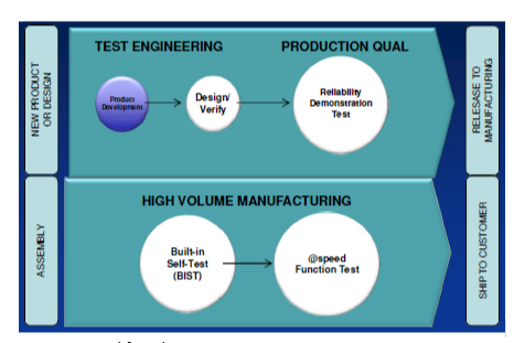
Figure 1. SSD lifecycle test stages

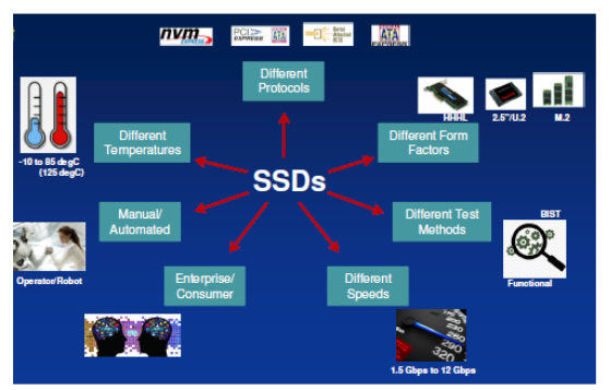
Figure 2. SSD test requirements include a wide range of variables.

The test requirements for SSDs comprise a wide range of variables that span many different engineering disciplines, as shown in Figure 2:

  • Different protocols – As we have examined in prior articles, SSDs make use of several different protocols, e.g., Non-Volatile Memory Express (NVMe), PCI Express (PCIe), Serial Attached SCSI (SAS) and Serial ATA (SATA), which vary significantly in functionality.
  • Different form factors – Testing chips is essentially the same process, regardless of IC shape or sizes. With SSD, form factors range from heavy, 8-inch PCIe cards to small, gumstick-sized M.2 devices, which are very fragile; the same system must be able to test each type of SSD.
  • Different test methods – As mentioned above, a robust system is needed to perform both BIST and functional testing.
  • Different speeds – This is a key requirement. System complexity and cost rise exponentially with increased device speed. With SSDs, speeds currently range from 1.5 Gigabits/second (Gbps) to 12 Gbps, with 16 Gbps (for PCIe Gen 4) and 22.5Gbps (for SAS 24) on the horizon.
  • Enterprise vs. consumer – This distinction is important because, at least intuitively, we can assume enterprise has a bigger budget for test given that the price tag for enterprise-level SSDs is about 50x that for consumer-level products.
  • Manual vs. automated – All SSD devices are being tested manually today, but as volumes increase, three things are happening: a) demand is growing at a rate that makes continually adding operators not economically feasible; b) operator error is growing in parallel with the number of operators; c) operator turnover is on the rise, creating a significant problem for manufacturers and pointing up the need to use robots on the line.
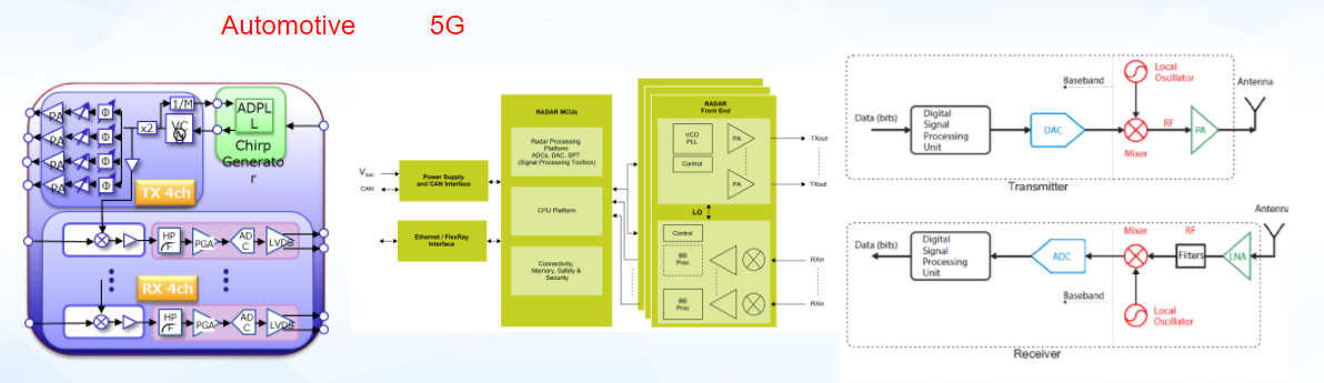
  • Different temperatures – Testing a device at ambient temperature is very different from testing it at -10°C. The automotive market is a prime example of this challenge – there has been a huge increase in electronic content, and test temperatures can range from -45°C to +125°C or more in order to ensure vehicle electronics can handle a wide range of climates.

ALL of these requirements have to be addressed – the question is, how? An all-inclusive test cell, a “Rolls Royce” approach, could be developed to do everything needed, but would be extremely costly, and customers would invariably pay for features they didn’t need. At the other end of the spectrum is an application-specific test cell, which is less costly, but also less flexible. Because this type of solution can only do one particular type of test, if an application changes, a new tester would have to be purchased.

Can one SSD test system accommodate all TTM needs, handle both engineering and manufacturing environments, address the wide range of test requirements, and grow with a customer as their test needs evolve?

An SSD test platform is the answer. Comprising a family of components that can be easily mixed and matched to create new products quickly, such a system allows customers to meet their needs exactly, with no scrimping and no waste. Tomorrow, if a faster module is needed to test PCI Gen 4, the customer only has to purchase that module – the rest of system (thermal, power supplies, and other constants) can be reused, which equates to 70-80 percent of the components. By only paying for what they need, customers can extend the life of the platform over 10-15 years or more.

Scalable, flexible, affordable test solution

Advantest’s offering in this space is its modular MPT3000HVM test platform. Figure 3 illustrates how easily the system can be reconfigured to accommodate a new mix of products with different protocols.

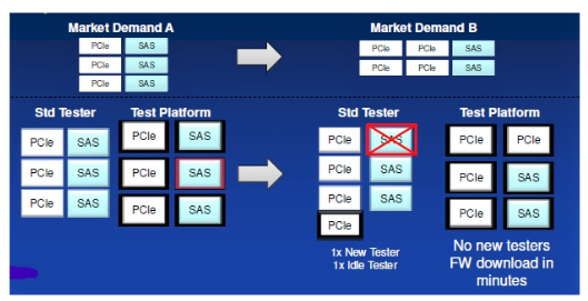
Figure 3. As shown above, a shift in protocol mix for the SSD devices to be tested can be completed in minutes with the SSD test platform approach.

The base unit for the MPT3000HVM, called the primitive, is the secret to the platform’s success. The user starts with this unit, and then adds in components as needed to accommodate specific test demands, e.g., full protocol test or different types of test electronics. The personality of the primitive changes according to what it incorporates. If, for instance, an engineer is using a tester full of primitives doing full functional and needs to switch to BIST, he or she can reconfigure the primitive and continue to use it, simply by changing the modules.

Similarly, different form factors can be easily accommodated. Figure 4 shows several racks of MPT3000HVM primitives running tests on different device sizes. Just by changing the device interface board, any type of SSD, or even chips, can be tested in parallel. Different primitives in same system – can test all at same time, w/different protocols, form factors, test electronics – all flexibility needed. System then becomes accumulation of primitive in 19-inch rack.

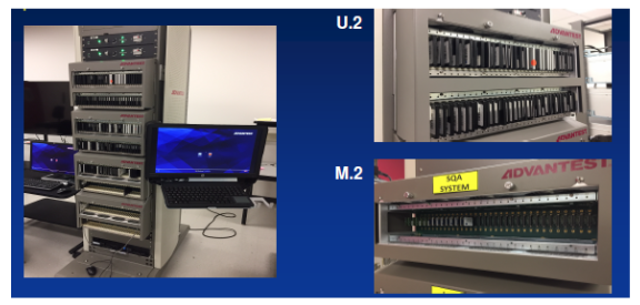
Figure 4. Multiple MPT300HVM primitives, each testing a different type of SSD, can be run in parallel within the same rack.

Unique capabilities

One crucial characteristic of the platform is its powerful, easy-to-use software, which can be easily applied to the different test stages. It employs a universal GUI, so the user always sees the same interface whether working on device verification, RDT or HVM. Whether different protocols, form factors, or types of tests are involved, it’s the same software, so engineers need to be trained only once. Because of the software’s capabilities, the same set of tools can be used across all test stages, which eliminates the problem of different people not being able to access different aspects of the software and this being unable to reproduce issues. Tools in the suite include stylus main, datalog & test flow control; graph characterization; power profile; production operator interface; oven control; and calibration & diagnostics.

ATE is traditionally focused on fault detection – i.e., the chip is tested and, in general, the result is pass or fail. Testing beyond this level is unnecessary with chip test because if the chip doesn’t pass, it’s not repairable, so it’s discarded. With SSD, we are learning that pass/fail testing is not enough because they can be repaired. Customers are now expecting not only fault detection but also fault location – they need to know the root cause of the failure, and need tools to help them do this. Advantest is developing these tools, which no other test provider currently offers, to enable a wide range of fault location capabilities, incorporating FPGA technology to detect deviations as they happen.

Summary

The SSD industry requires a test platform that optimally addresses shortening time to market, ever-decreasing SSD product lifecycles, and the need to keep test costs under control even as device performance, density and variety all increase. Advantest’s proven MPT300HVM was created to resolve all these challenges, delivering a flexible, scalable platform that can handle testing a wide range of device types, speeds, form factors and other variables simply through swapping out modules to create a configuration that meets the user’s needs.

This also includes handling a variety of protocols. SATA still has high usage for low-end consumer SSD devices, but the world is moving to PCIe, both standalone and as a transport mechanism for NVMe. PCIe Gen 4 is coming soon, as is SAS 24, and the Advantest solution can handle them all, leveraging the company’s long tradition of creating platforms in a system-level offering.

Read More

Posted in Top Stories

5G Lessons Learned from Automotive Radar Test

By Roger McAleenan, Director, Millimeter-Wave Test Solutions, Advantest America

Situated between microwave and infrared waves, the millimeter-wave spectrum is the band of spectrum between 30 gigahertz (GHz) and 300GHz. It is used for high-speed wireless communications and is widely considered as the means to bring 5G into the future by allocating more bandwidth to deliver faster, higher-quality video, and multimedia content and services. Automotive radar is the entry point into millimeter wave for testing purposes.

Automotive radar has been evolving for the past several years, with Tier One companies producing and developing designs for a variety of different applications. As automotive is considered one of the key vertical markets for 5G technology – others include mobile broadband, healthcare wearables, augmented and virtual reality (AR/VR), and smart homes – radar systems in vehicles can provide valuable insight into the other millimeter-wave applications.

The 5G standard promises new levels of speed and capacity for mobile and wireless communications with greatly improved flexibility and latency compared to 3G and 4G/LTE technologies. However, its unique chip structures will create new challenges for test and measurement. By understanding the limits of test equipment, systems and hardware, we can better address the practical aspects associated with delivering on the promise of this technology.

Test and measurement challenges
From a measurement perspective, 5G and auto radar have functional characteristics in common that need to be measured, such as signal blockage, radiation interference and beamwidth selection. Another aspect is loss of signal penetration, an area where radar has an advantage over optical techniques that can be confounded by rain or snow. The band assigned to automotive radar, 76-81GHz provides greater accuracy in range resolution, and is sandwiched between point-to-point (P2P) bands on each side.

The challenges to be addressed in 5G test are similar to those associated with automotive radar, as well. Challenges in millimeter-wave applications include:

  • Handling multiple port devices economically
  • Providing features and testing optimized for characterization and production
  • Over-the-air environment due to packages with integrated antennas
  • High-port-count switching/multiplexing (4×4, 8×8, etc.), often in the same device
  • High levels of device features on a die– MCU + memory  + radio + high-speed digital

Multiple antennas improve power efficiency since more energy is pointed where it needs to be, and with steering, multiple targets can be tracked. This provides improvements to the capabilities and applications expand broadly to “surround” safety features, vehicle-vehicle coordination/communication.  The increased complexity in devices extends up to multiple combinations of transmit and receive.  This functionality will significantly improve vehicle-to-animal/human/object recognition and avoidance, as well as tracking more targets simultaneously.

Transceiver design is important, and they can be optimized as required as a low- or zero-intermediate frequency (IF) design. Automotive and 5G radios look nearly the same, with the similar IP blocks, e.g., phase shifters, local oscillators, RF amplifiers and mixers (Figure 1). The primary distinction is 5G radios’ modulation capability. Both may include up and down conversions, but for 5G, the market is looking for information bandwidth increase. This is actually pretty difficult from a test perspective because it requires elaborate analog equipment like high-performance oscilloscopes. This aspect is still a work in progress.

Figure 1. Transceiver design in automotive and 5G systems is highly similar.

Four main millimeter issues and considerations must be addressed in auto radar. This applies to 5G as well in that these four problems – rain attenuation, Fresnel zone, path loss, and ground reflection – are all problematic, whether you’re driving a car or the equipment is on a tower. Figure 2 shows all the areas in which radar is being used in cars, and further underscores the challenges associated with effective testing of these systems from a system level perspective.

Figure 2. Radar zones in vehicles continue to multiply as automated content increases.

One way to address some of the operational millimeter challenges is through beamforming. This is a technique that focuses the radar transmitter and receiver in a particular direction. Beamforming can be passive or active, although the former is limited in its effectiveness. Active RF beamforming, the increasingly preferred approach, will be gamechanging: it enables tracking multiple objects, both moving and static (people, vehicles, buildings, etc.) at various speeds, simultaneously. This allows auto radar to actively steer the beam toward objects and track them independently. Because the beam can be positioned with so many possibilities, testing in this way is currently a rhetorical question, although several automakers are working on solutions. For 5G, the beams would normally point either to other towers or to individual handsets and be able to track them. Basestations will have antenna arrays that can be steered to track people with 5G handsets – this will be an essential success factor in achieving the information bandwidth promise.

Test lessons learned
Advantest’s automated test equipment has been deployed for testing automotive radar for more than four years, testing from 18GHz to 81GHz, including wireless gigabit (WiGig) test in the 60GHz range, which may also be applicable to 5G.

At the moment, the focus remains on device test, but this is changing. Millimeter-wave applications provide an ideal opportunity to move away from component-level test and more toward higher-level models and end-to-end system-level testing. Figure 3 highlights the growing trends associated with system-level test. With that noted, here are some key lessons learned from Advantest’s work in the auto radar space, using its proven V93000 test platform.

Figure 3. Demand and opportunity for system-level testing is on the rise.

  1. Power accuracy is critical. This will be very important to understand and address because, as we move closer to built-in self test (BIST), the device must be able to measure accurately the power it’s generating. Right now, we’re still learning how to get RF CMOS and BIST working together to give an accurate power measurement.
  2. Metrology is difficult. Given the various connectors and waveguides that must be navigated, there are few reliable ways to perform accurate metrology of fixtures, connectors, loadboards, and other components. Also, there is the issue of system degradation – every time a new part is tested, it degrades slightly due to the materials used, and over time, the sockets or membranes that begin to deteriorate. In addition, when something finally needs to be changed out on the test system, recalibration must be performed, and that can cause a slight change in measurement results when combined with the degradation issue.
  3. Limits need to be established. As devices grow more complex and better – and as efforts are made to extend radar range – two key factors come into play:
    • Phase noise – This key parameter on RF signals affects performance of radio systems in various ways. It’s important to understand at what point phase noise begins to impact performance    and the cost-benefit.
    • Noise figure – This measure of the degradation of the signal-to-noise ratio, caused by components in an RF signal chain, is essential to making radar more effective. The key question in this regard is, what’s the smallest signal I can see (relates to dynamic range)?
  4. Millimeter “anything” is expensive. Currently, there are significant costs associated with millimeter-wave technology that will likely decline over the next few years. In the meantime, some chipmakers are trying to implement millimeter-wave technology for smaller end products, such as radar distance measuring devices, but they can’t build them because they can’t figure out how to test them economically on a small scale. The solution may rely on future technology that is still being developed.
  5. Test engineering knowledge is scarce. This is perhaps the most critical factor of all – hence, saving it for last. The number of engineers working in millimeter technology is relatively small, and companies wanting to enter the space can’t simply materialize engineers versed in radar technology to help them with product development – particularly when the primary emphasis in most engineering programs is digital technology, rather than analog/RF. This means that talent is expensive, which can put a real damper on what companies are able to do. We need competent engineers to be trained that are strongly motivated and passionate about millimeter-wave.

Summary
Automotive radar technology is here now, and while it’s currently being seen primarily in premium-brand vehicles, the goal is to bring down the unit cost so that it becomes standard equipment throughout the automotive industry. To do this, a number of challenges must be addressed, including solving of the complexities associated with testing. Advantest is strongly committed to this market and in taking a leading role in finding these solutions and applying them to other millimeter-wave applications as the market continues to grow – including the fast-emerging 5G.

Read More

Posted in Top Stories

Storage Evolution Driving Growth of System-Level Test

By Colin Ritchie, Vice President, System Level Test Business Unit, Advantest,
and Scott West, Marketing Manager, System Level Test Business Unit, Advantest

Thanks in large part to the booming mobile market, global demand for storage capacity continues unabated. Gartner indicates that solid-state drive (SSD) shipments are on pace to top 370 million units by 2020, while Research & Markets forecasts that the client SSD market alone will grow at a compound annual rate (CAGR) of 36 percent between 2017 and 2021. With this growth comes an increased drive for performance, requiring implementation of new/updated storage protocols.

Currently, the market supports three primary storage protocols. Serial ATA (SATA) and Serial Attached SCSI (SAS) are still in use – the latter, for enterprise applications in particular – but there is a migration towards the newer PCI Express protocol. Increasingly, SSD makers are choosing the latest incarnations of PCI Express: PCIe Gen 3 and the forthcoming Gen 4. In addition, often used with PCIe is Non-Volatile Memory Express (NVMe), a storage interface/protocol developed especially for SSDs by a consortium of prominent vendors.

This shift toward newer, faster protocols creates an associated need for improved test speed and accuracy. Driven by these and other associated demands, the test industry is moving up the value chain, from component-level to module-level to system-level testing. System-level test (SLT) is not only different from classical component test, but also more difficult, creating some key challenges to be addressed.

In-house solutions no longer viable

Storage SLT is still in its infancy, much as memory test was three decades ago. However, an SSD’s state machine has virtually an infinite number of combinations that must be tested effectively without an infinite amount of time available to perform brute-force iterations. While ICs have a set number of vectors or memory patterns to be run, SSDs feature a huge number of constantly changing states – factor in unplanned events (such as power-cycling), and the result is a huge number of cases that are difficult to cover. SSD providers can’t address every eventuality – but they must be able to ship product to their customers with absolute confidence it will work.

Traditionally, storage makers have created their own test solutions in-house because of the high degree of customization required – in addition, no commercially viable solution was available that could meet their needs. However, as the pace of change and growth in the storage market continue to accelerate, these companies have come to recognize that they cannot keep developing their own internal test solutions – they will end up spending more time, money and engineering resources on developing the ability to test their products than they will on developing the actual products. Greater expertise is needed to test the higher performance devices while maintaining a consistent solution across increasing production volumes is. Faster product cycles make this an even more pressing issue.

SSD product lifecycles have collapsed down from two years to as little as six months. In the time it would take for a storage maker to develop its own custom test solution, the product for which it’s intended will have already peaked and be on its way to obsolescence. Reinventing the wheel with each new product is simply no longer viable. Most of these manufacturers have thus made the decision to implement commercial test solutions.

Advantest leading the way in SLT

This creates a substantial opportunity for Advantest. Storage is a market in which Advantest has purposely become a fundamental enabler of growth, as well as a quality arbitrator. The company is committed to helping customers wean themselves away from in-house-developed test solution, with its MPT3000 platform allowing customers to focus on their core competencies. As an example, an executive with a leading SSD supplier that previously focused on traditional flash memory components, recently acknowledged his company’s decision to align itself with Advantest. They needed a partner they could depend on to develop the volume of test solutions needed to meet customer demand in the face of collapsing time-to-market (TTM) windows.

The platform strategy Advantest has refined in the ATE industry applies directly to system level test. By developing modular components for the common platform, both standard solutions as well as targeted custom solutions can be configured, cost effectively. When a custom need arises, the platform components provide 80 to 90 percent of the solution, allowing efficient use of Advantest’s expertise to adapt the solution to a specific configuration. Each adaptation extends the platform so storage makers can benefit, through working with Advantest, from their peers’ shared knowledge and experience.

Going back to the shortened product lifecycle, when the TTM window is only six to nine months, missing one design win can greatly impact a storage maker’s business. A three-month delay in the product cycle can translate to a 10-percent market-share hit – e.g., a loss of $100 million from a $1 billion SSD revenue stream is clearly significant! Advantest’s goal is to take test off the table for customers when competing for business – the tester should never be a gating factor in this regard. By implementing the modular MPT3000 platform, they can compete on their product differentiation

Another key challenge storage makers face is of the need for flexibility in terms of manufacturing floor configuration. They spend significant amounts of money building their factories based on their business forecast, customer demand and production plan. However, as we’re seeing increasingly, these plans can change dramatically in a short time, necessitating flexible solutions on their factory floor that can be retooled easily, efficiently and cost-effectively to meet changing customer demand and/or when moving from one product generation to the next. The MPT3000’s FPGA-based test architecture enables quick changeover, maximizing utilization and production output for customers.

Advantest’s portfolio today comprises end-to-end test – from components through modules to systems. The MPT3000 platform is focused on system-level test for the SSD market, and is serving as both a test case, if you will, and a learning platform for further SLT efforts within the company. A previous GO SEMI article delved further into its protocol test capabilities: https://www.gosemiandbeyond.com/applying-flexible-ate-technology-to-protocol-test-and-the-ssd-market/

Other past articles that shed light on Advantest’s system-level test efforts include last issue’s piece on SLT for embedded NAND flash memories – https://www.gosemiandbeyond.com/system-level-test-essential-for-fast-growing-embedded-nand-market/ – and a prior interview with Artun Kutchuk of Advantest Group’s W2BI business, which provides wireless test automation products for the mobile and IoT space: https://www.gosemiandbeyond.com/out-of-the-lab-and-into-the-field-making-iot-device-testing-portable/.

We are interested in learning about the kinds of SLT challenges you face – whether in storage or elsewhere. Please feel free to comment below, or send an email to Scott.West@Advantest.com, to share your knowledge and expertise.

Read More

Posted in Top Stories

A Smarter SmarTest: ATE Software for the Next Generation of Electronics

By Rainer Donners, Product Manager, Advantest Corp.

The complexity of the ICs being designed into consumer and communications devices continues to increase. The 10-nanometer (nm) node is here, and some chipmakers are already beginning to turn out 7-nm devices. With smaller transistors that pack more and more functionality on a single chip, the complexity of test programs is increasing apace with that of the ICs themselves.

These ICs are used in end products such as smartphones, Internet of Things (IoT) devices, computer and gaming products, and they are ‘multi-domain,’ i.e., they contain digital, DC, analog and radio-frequency (RF) circuitry all on the same chip. Developing efficient test programs for these multi-domain ICs within a shorter time to market (TTM) is becoming a challenge.

To overcome this challenge, Advantest has introduced SmarTest 8, the latest version of its SmarTest software, developed to support the V93000 test platform. It’s important to note that both SmarTest 8 and SmarTest 7 will coexist on the V93000 Series for the next decade, enabling customers to use the version best suited to their test needs and business requirements. SmarTest 8 works with all V93000 Series test cards introduced since 2011; see Figure 1 for cards supported by SmarTest 8.

Figure 1. V93000 Cards supported with SmarTest 8

SmarTest 8 features a host of new capabilities that will enable engineers who must deal with highly complex test programs to achieve superior parallelism and throughput. The new software’s many benefits include:

  • Faster test program development
  • Efficient debug and characterization
  • Higher throughput, earlier, due to automated optimization
  • Faster time to market
  • Ease of test-block reuse
  • Efficient collaboration

SmarTest 8 unifies multiple different tools within the SmarTest Work Center (SWC) environment, delivering a state-of-the-art look and feel and an entirely new design to ensure ease of use; see Figure 2.  Let’s take a look at some of the key SmarTest 8 concepts, features and tools that will allow users to reap the new product’s benefits for their test programs.

Figure 2. SmarTest 8 comprises a suite of tools designed to simplify and optimize test program development and debug

Operating Sequence
Advanced multi-domain devices consist of multiple different functional blocks. Typical block types include an RF block for transmitting/receiving phone signals, a protocol-ware (PA) interface to condition the device, analog blocks for microphone use and playing music, and/or digital blocks for processing.

Testing one functional block, e.g. the RF block, typically requires ‘assembling a test’ out of multiple pieces, e.g., starting an analog stimulus signal, conditioning the device with digital signals, and starting one or multiple RF measurements. Figure 3 provides an example, with three RF tests displayed in the Operating Sequence View.

Figure 3. Operating Sequence View, displaying an example RF test

The Operating Sequence is designed to easily assemble the multiple ‘test pieces,’ with precise synchronization where needed. These test pieces are typically patterns, protocol transactions, or ‘actions.’ Actions can be DC stimulus changes (e.g., stepping up a ramp), DC measurements, analog stimulus and measurements, or RF stimulus and measurements – to name some examples.

In addition to easy test setup, the Operating Sequence supports intuitive debugging; the screen view in Figure 3 displays exactly what has been executed.  Interactive changes during debug are well supported – as the second blue block in the figure indicates, inserting an additional transaction into one PA block changes the length of this conditioning block. The SmarTest 8 software automatically ensures that with the next execution of this test, subsequent actions (like cw2 and measurePower in the screen view) are shifted and retain their synchronous start.

Additionally, the Operating Sequence contributes to fast throughput. Multiple measurements can run in parallel, per Figure 3, in which two RF ports are tested concurrently. In addition, the execution of an Operating Sequence is done entirely via the unique test-processor-per-pin hardware of the V93000 system. No software or workstation interaction is required.

Overall, the Operating Sequence, with its new functionality, ease-of-use and optimal throughput, helps enable shorter TTM. This unique tool and concept are unavailable in competitive offerings.

Modular Test Program Structure
Test programs are complex, consisting of up to multiple thousands of tests for the different blocks of the device. The structure of the test setup data of SmarTest 8 is designed to easily deal with this complexity: SmarTest 8 incorporates the concept of subflows. Subflows as part of the testflow tool are established in the ATE software already. SmarTest 8 adds the new component that setup data can be structured and stored in separate and independent ‘subflow’ directories.

This capability enables multiple unique advantages:

  • Teams can work on their own subflows independent from other teams, so collaboration is easy.
  • No manual ‘merge’ effort is needed, as merging of the subflows is automatically performed by SmarTest 8.
  • A complete (proven, debugged) subflow can be reused within multiple test programs of a device family. Reuse here refers to one single source of the subflow, not the ‘copy/paste’ approach typically used today. The latter creates test program maintenance challenges that are prevented with SmarTest 8’s re-use/single-source approach.

By making development and debug faster, easier and far less complex, the modular test program structure ultimately contributes to reduced TTM and time to quality (TTQ).

Test-oriented Use Model via Instruments
Many test systems’ use model is tester- or hardware-centric – it requires the user to learn how to program the tester in order to achieve the needed tasks. SmarTest 8 moves away from this model, allowing the user to focus on the test, not the tester.

With SmarTest 8, the user ‘thinks’ in terms of using instruments for his/her test tasks. Figure 4 shows example instruments and their respective implementations of the tester hardware cards.

Figure 4. Simplified use model via SmarTest 8 Instruments

These instruments are then programmed via properties and actions; see Figure 5 for an example setup for two VCC signals.

Figure 5. Level specifications for VDDA and VDDD signals

This level specification is identical for all DC instruments in SmarTest 8. When setting up the test, the test engineer will use the level specification for all suitable hardware, which could be a DC Scale DPS128, a parametric measurement unit (PMU) of a Pin Scale 1600 or a PMU of a Wave Scale MX card.

This test-orientation and tester, respectively, hardware-abstraction is consequently used in SmarTest 8, for test setup descriptions, application programming interfaces (APIs), access to results, and in debug tools. This makes the software intuitive and easy to learn, and the test programs are easy to develop, understand and debug, further lightening the burden for the test engineer.

In summary, after several years of development, optimization and beta test, SmarTest 8 is now ‘ready for prime time.’ It is installed at numerous customers, both in test program development and in high- volume manufacturing. SmarTest 8 delivers new benefits that, together with the proven V93000 platform, meets the test needs for the next/newest generation of advanced multi-domain, multi-core ICs. As part of the V93000 platform, it will be continuously expanded to enable even more capabilities and to make test engineers more efficient.

Read More

Posted in Top Stories

W2BI in the Spotlight at Mobile World Congress with New Test Automation Products for the Wireless Market


Advantest, together with W2BI ‒ an Advantest Group company that provides test automation products to help customers quickly launch high-quality smart devices ‒ showcased their newest test platforms for the wireless electronics market at the 2017 Mobile World Congress (MWC) in Barcelona, Spain.

The world’s most expansive exhibition for wireless technology and mobile devices, MWC serves as an annual springboard for many of the next year’s biggest announcements and rollouts of smartphones, tablets and other connected devices. To give you an idea of scale, MWC this year drew more than 108,000 attendees from 208 different countries and boasted approximately 2,300 exhibiting companies.

Within its booth, Advantest featured a suite of products for the mobile communications and Internet of Things (IoT) markets. This included the EVA100 tester, designed for highly efficient evaluation and measurement of analog/mixed-signal ICs, and W2BI’s portable Micro Line Tester (MLT™). This newly introduced system can leverage cloud technology to support testing of LTE-M devices – while effectively lowering the cost of testing smart devices and IoT-based technologies during their development and production life cycles.

MWC provided a valuable forum for Advantest to connect with customers and potential customers to share our perspective on the future of test in the wireless space, and to obtain their thoughts about where IoT test is headed. By most indicators, the space is only going to continue heating up.

Recent market estimates project a whopping 29 billion connected devices by year 2022, and 18 billion connections targeted at wide-area and short-range IoT devices (Figure 1). If we are to capably accommodate this growth, it is critical that the industry address key issues currently challenging wide-area IoT device implementation, including:

  • Lengthy certification process
  • Complex cellular tests used to ensure Safe For Network (SFN) operations
  • Expensive lab equipment for lab testing
  • Non-scalability of test solutions
  • Travel to remote sites to perform live network tests is costly and time consuming
  • Lack of certification knowledge and experience by IoT device makers new to the market

Figure 1. Connected devices are expected to achieve a combined CAGR of 10% between 2016 and 2022. Ericsson Mobile Report November 2016

Some of these challenges can be tackled by simplifying conformance and certification processes, as well as eliminating duplicate tests across the test lifecycle of chips, modules and end products (e.g., wearables, alarm panels, telemetry, and smart homes). Others, however, will require a change in the way the tests are conducted.

W2BI’s new portable all-in-one Micro Line Tester (MLT) platform tackles many of these issues head-on with several key benefits (illustrated in Figure 2):

  • A portable and expandable cloud-managed test platform that reduces time to market;
  • Automation capabilities that have the domain knowledge built in, thus allowing developers to focus on their specific product requirements;
  • Validated industry-standard automated tests downloadable over the cloud directly at the customer site, enabling device pre-certification while reducing travel and lab costs;
  • Pre-defined device profiles to efficiently automate tests across multiple device types (modules, smartphones, IoT products, etc.) without having to customize and adapt tests for each;
  • Ability to expand within a small footprint to adapt to 5G requirements.

Figure 2. W2BI’s portable MLT platform enables onsite testing of mobile devices, greatly reducing test times and costs.


The MLT platform is currently offered in three different modes:

Standalone – Used to conduct ad-hoc tests such as basic device operation, network connectivity, network aggression, data throughput, Voice-over-LTE (VoLTE), SMS, LTE to WiFi handover, and others. The target areas are mainly R&D development processes, and isolation and troubleshooting of post-release device issues.

Developer – Used to create test automation scripts across the network emulator components (radio, packet core, IMS, application server, etc.) and the devices under test, and to collect test metrics for use in analytics. Target areas are primarily QA processes, stress testing, and returns and repair processes.

Conformance – Used to perform automated conformance and certification tests for devices that need to be deployed on wireless networks in accordance with industry standards or operator-specific requirements. The target areas are mainly pre-certification tests, network safe tests, and conformance tests.

W2BI’s MLT platform is currently deployed at a US Tier-1 wireless operator, performing conformance tests on smartphones, and IoT modules and products. The Micro Line Tester is also undergoing multiple trials across test labs, module manufacturers and smartphone OEMs using both the standalone and developer modes. Shipment volume is expected to pick up toward the second half of 2017, when mobile operators begin fully deploying LTE-M and NarrowBand IoT (NB-IoT) on their networks.
As W2BI continues to develop new products that help to enable the growth of the mobile device market, expect to see technologies and products that address new protocols, including LTE-M and NB-IoT, called a game changer for the IoT industry because it extends LTE’s market reach. By allowing LTE to cost-effectively support lower data-rate applications, LTE-M is being touted as a good fit for low-power sensing and monitoring devices such as health and fitness wearables, utility meters, and vending machines, among others.


Read More

Posted in Top Stories

RF Test Requirements Driven by Emergent Package Integration

By Judy Davies, VP, Global Marketing Communications, Advantest Corp.

The many connected tasks we perform every day using advanced mobile products, such as smartphones, tablets and notebooks, are enabled by a somewhat dizzying array of wireless standards. These range from Long Term Evolution (LTE), LTE-Advanced, LTE-A Pro and LTE-M smartphone standards, to ZigBee, Bluetooth, GPS and Wireless Local Area Network (WLAN). The requirements and performance criteria for these wireless technologies differ according to their application – many of which revolve around the Internet of Things (IoT) – creating a host of technological challenges, including those surrounding packaging and test.

Before they’re packaged, assembled and shipped, RF-based system-on-chip (SoC) devices built on the current Third-Generation (3G) and Fourth-Generation (4G) LTE broadband standards are fully tested and characterized, as are both the RF and analog baseband transceivers employed in these applications. In addition, the Fifth-Generation (5G) standard is forthcoming, with its promise of new speed and capacity levels, lower latency and greater flexibility than LTE, but its new encoding technologies and chip structures will require new production, packaging and test technologies. The anticipated needs of next-generation wireless networks are in fact shaping the next generation of RF test equipment.

The proliferation of advanced packaging methodologies – e.g., fan-out wafer-level packaging (FOWLP), multichip packages (MCPs), through-silicon vias (TSVs), embedded passives and actives, and systems-in-package (SIPs) – also plays a key role in growing RF test requirements. While it’s not clear which of these package types will dominate going forward, they are all impacting how steps such as wafer sort, final test, packaging test, burn-in and others are performed.

Packaging integration is key

With respect to packaging for RF transceivers, as well as for RF chips in general, every RF device comprises a large number of passive components, such as capacitors and inductors, allowing its use as an end product. Therefore, packaging integration is essential to turning RF silicon into a device that can easily communicate with the antenna in the RF space. The three primary components of integrated packages are as follows:

  1. Embedded passive devices – embedded passives are essential to making useful RF end products based on RF chips, and they are a key value-add provided by outsourced semiconductor and test (OSAT) houses.
  2. Multiple standards – many standards are integrated into today’s mobile phone, so it’s critical to implement an RF set that can handle these various standards. Multi-purpose RF devices switch modes when the user switches location, which makes them more both complex and more challenging to test.
  3. Multiple antennas – essential to ensuring that a device will work no matter how it is held by the user, multiple antennas are increasingly being employed within wireless products.

OSATs are competing with each other to unify all of these components into a viable RF package. Flexible, scalable automated test equipment (ATE) is a fundamental requirement for thorough testing of these devices. This includes both early die sort and final test once the peripherals and passives are attached within the integrated package. Regardless of the packaging technique, more rigorous functional test and more robust compliance test are essential – highlighting the importance of precision, capability and bandwidth in new equipment. Combining a tester-per-pin architecture – such as the Advantest V93000 platform – with massive parallelism is one approach to ensuring the high performance and high utilization chipmakers need to get their products to market more quickly, and at a lower test cost.

Lessons of evolution

Much discussion is under way with respect to how packaging impacts the way test cards are developed – similar to what happened with printed circuit boards (PCBs) a decade or so ago. Back then, board test was big business. Virtually every electronics company created its own PCBs, using its own components, and put them into widely available electronic products. Since then, the PCB chain has consolidated, with a small number of very large subcontract manufacturers putting out PCB assemblies.

Package integration also faces a similar major change – more and more technology is being integrated into a single piece of silicon. PCBs are becoming smaller and smaller, or being eliminated entirely, as in products like the Apple Watch. As this industry shift continues to evolve, the line between chip and package is blurring – particularly with more intelligence being put into the package (which was once merely a “dumb” housing for the circuitry). Competition for business between PCB load and assembly houses and OSATs is also on the rise. What will be chosen depends on whether the customer needs one-stop shopping, which OSATs claim they can provide, or if they’d prefer to tap more traditional PCB load/assembly providers for the board.

A clear winner in this space is chip-scale packaging—particularly, wafer-level chip scale packaging (WLP). The majority of the building blocks in today’s smartphones are WLPs. Eliminating the classic substrate and consolidating the flow of material into wafer-level scale allows two goals to be addressed in one step: miniaturization (making the package ultra-thin) and cost scaling—a key requirement for high-volume manufacturing.

Reducing costs through parallelism

Signal transmission and reception in 5G systems will also impact future test equipment requirements, which are further complicated by the projected billions of IoT devices with different types of sensors using low-power wireless links to connect to the internet. These sensors will be located all around us, letting us access, interact with and control our environment no matter where we are – at home, at work or in transit.

Current RF testing solutions, which typically require multiple cards and a separate calibration kit, employ a fan-out architecture with shared subsystem resources. This means that devices with multiple frequency paths are actually tested in serial within the device, rather than in true parallel test mode. It also means that only one RF standard at a time can be tested per site.

One new approach is Advantest’s V93000 channel card called Wave Scale RF that omits shared resources, condensing four independent RF subsystems into one integrated card with a high degree of parallelism – up to 192 ports for parallel testing of multiple RF device types. This removes the limitations placed on test speedup, cutting test times in half, and enabling device parallelism of 16, 32 or even higher. These cards, together with the complementary Wave Scale MX (for mixed-signal) cards, can simultaneously test multiple standards or multiple paths within each RF device, achieving both in-site parallelism and high multi-site efficiency. Devices can be tested two to three times faster than with other solutions – greatly reducing the cost of test. This is a key requirement for OEMs and fabless semiconductor companies that need to quickly bring RF-enabled devices to market in high volumes.

Wave Scale MX is optimized for analog IQ baseband applications and testing of high-speed DACs and ADCs. As with Wave Scale RF, it omits shared resources, delivering parallel, independent operation of all 32 instruments controlled by a hardware sequencer. This is critical for semiconductor and telecommunications chip leaders, who face a 10x reduction from what they sell into cell phones to what they can charge in the industrial area. From a security perspective, the key challenge is that the functionality must ensure safety, while data is directed into the right channel and properly authorized – thus, the security requirement is even higher than for phone line communication.

In fact, security is one of the biggest concerns about the IoT– silicon providers will be under tremendous pressures to guarantee that their products adhere to industry reference standards. Whether these standards will be as stringent as those adopted within the automotive and aerospace industries remains to be seen, but they will most certainly need to be stronger than consumer-grade standards.

These requirements further underscore the need to rigorously and robustly qualify and test devices, as well as manufacturers’ need to ensure long-term device reliability (based on user demand). This means that the pressure to deliver high-quality devices at the lowest possible investment cost will continue to mount, requiring methodology breakthrough and further justifying the need for advanced equipment that can fully leverage these changes in the RF device landscape. With the new Wave Scale card, OEMs can address their bottom-line manufacturing and test cost pressures while ensuring a solution is in place with the flexibility and headroom to accommodate the requirements of the future.

Read More