Pages Menu
TwitterRSSFacebook
Categories Menu

Posted in Top Stories

System-Level Test Methodologies Take Center Stage

By Fabio Pizza, Business Development Manager, Advantest Europe

Note: System-level test (SLT) continues to expand in importance throughout the industry. In past newsletters, we have published articles looking at the company’s efforts in this space, primarily for the storage market, as it offered the most immediate opportunity for implementing SLT. Now, rising industry demand, driven by mission-critical applications, has put SLT at the forefront for Advantest company-wide.

Because electronic systems for all applications in end-user markets must provide the highest possible reliability to match customers’ quality expectations, semiconductor components undergo multiple tests and stress steps to screen out defects that could arise during their lifecycle. Due to new semiconductor devices’ increasing design complexity and extreme process technology, increased test coverage is needed to meet stricter quality requirements.

To solve this problem, system-level test that mimics a device’s real-world operating conditions is increasingly being adopted as one of the final steps in the production testing process for complex systems-on-chip (SoCs). In the past, system manufacturers typically implemented SLT on a sample basis, plugging devices into systems to check that the devices would function in an application. Semiconductor companies have now adopted SLT methodology throughout the test process to increase test coverage and product quality for mission-critical applications (Figure 1).

Figure 1. Advanced technology is driving changes in test requirements, creating the need for integrated SLT approaches throughout the test flow.

Advantest provides customers with an end-to-end test solution, from ATE to SLT, in line with the company’s Grand Design, created to ensure that Advantest remains at the forefront of our industry. The central vision of this corporate-wide plan is for Advantest to strengthen its contributions to customer value in the semiconductor business by enriching, expanding and integrating our test and measurement solutions throughout the entire value chain, as shown in Figure 2.

Figure 2. System-level test is crucial to the mission of Advantest’s Grand Design – “Adding Customer Value in an Evolving Semiconductor Value Chain.”

Recent market and financial analyst commentary supports Advantest’s view that SLT is the way of the future and that our expertise in this area provides new growth opportunities. Following our briefing on SLT in June, VLSI Research CEO Dan Hutcheson wrote in the July Chip Insider newsletter that the session prompted him to think that SLT “may well be the next major revolution in test equipment…The essential argument is that test is becoming a more important enabler going forward versus its decades-long position as a cost center to be pushed down. What has changed is the increasing complexity of SoCs and SiPs, the introduction of advanced packaging, chiplets and high-bandwidth memory.”

A July report issued by Mitsubishi UFJ Morgan Stanley Securities noted, “Recently, we have seen an increase in demand for the testing of semiconductor devices at the system level, in addition to the wafer and package levels, as temperature and voltage fluctuations place them under severe stress when they are used in applications such as data center servers. There is similar testing demand from the makers of storage and mobile devices and automotive systems, and we believe this will provide a fresh source of growth for Advantest.”

The mega-markets shown in Figure 3 represent mission-critical applications for SLT. Advantest has established itself as a leader in SLT solutions for the computing, memory and storage, and mobile markets, with systems in production performing massively parallel SLT for these applications, and we continue to sustain and grow our leadership in these areas. The automotive space is a new domain where we are now focused on expanding our SLT business.

Figure 3. Memory & storage, computing, mobile and automotive markets are the four mega-markets driving system-level test.

We are already working with leading customers in Europe, the U.S. and Japan who are seeking automotive SLT solutions, primarily for advanced driver-assistance systems (ADAS) and infotainment. One customer developing automotive microcontrollers is experiencing some returns from the field that were not detected in the standard traditional final test steps. They must expand test coverage to close these gaps. Unlike with mobile phones, one failure per million devices can be disastrous or even deadly in the automotive space, so chipmakers must be able to ensure the quality of their devices when installed. Quality over time is particularly important, as the final product lifetime can be 10 years or more.

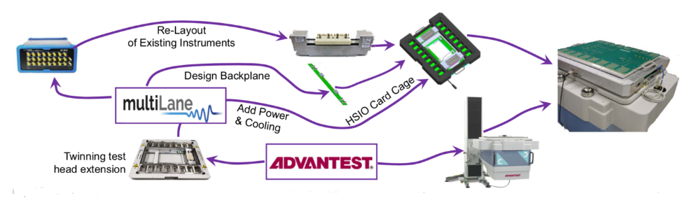
Advantest’s SLT capabilities 

Advantest SLT test cells are based on modular building blocks, as shown in Figure 4. The first step involves collaborating with the customer to develop a customized application board to ensure accurate reproduction of the system environment’s conditions while optimizing for high volume production. Next comes automation, the degree of which differs, depending on target production test time and required parallelism. High-volume devices require a much greater amount of parallel testing to meet cost-of-test objectives.  

Figure 4. Advantest’s SLT approach involves modular test-cell building blocks.

The third piece is the thermal environment, which depends on device power and test stress requirements. As the figure indicates, Advantest offers a range of thermal-control technologies: pure passive ambient, tri-temperature active thermal control (ATC) with air cooling, and tri-temp ATC with liquid cooling using rapid temperature switching methods (RTS). Devices are tested independently at controlled temperature. As newer-generation devices tend to consume high power, each needs its own thermal controller and sensors to ensure stable test temperature and prevent device failure. Examples include HPC devices, which can consume over 300W each. ADAS applications require a great deal of power to process data generated by vehicle cameras. When tested, these automotive processors must be heated up without exceeding the maximum junction temperature of 125-130 degrees.

Our SLT solutions also share a common software framework called ActivATE™, which enables test programs to be reused easily. ActivATE™ comprises an integrated development environment (IDE), a test sequencer, and a device manager, and allows test engineers to rapidly create and deploy test programs using standard programming languages.

These building blocks have been assembled by combining our existing proven SLT offerings with some strategic acquisitions. In late 2018, the semiconductor test division of Astronics became part of Advantest, adding massive parallel test solutions to our arsenal. Parallel testing is essential for minimizing the cost of test for SLT, as is mitigating handling limitations of pick-and-place technology. Astronics developed systems with slots that can test hundreds of devices in parallel with virtually 100-percent multi-site test efficiency.

This is a must-have for high-volume manufacturing of mobile and high-performance computing (HPC) products. While automotive volumes are not as high, the electronics in cars are increasing, so here, the requirement is covering multiple variations of devices – i.e. a main design with some customization. This requires the ability to test more small lots with diversified packages and variations of a main device family, and we can now handle these different packages and fully parallel-test them in one system. 

Exemplifying our building-block approach, we developed in less than one year the 5047, our dedicated SLT test cell consisting of our standard M4841 logic handler docked to a 547 SLT system to perform SLT for lower-volume automotive devices with limited parallelism requirements (x8 or x16). These devices run at low power with short test times (tens of seconds to a few minutes), so the standard pick-and-place handler can cover them satisfactorily. Its tri-temperature thermal environment (-55 to +155°C) supports both hot and room temps; cold temps require some further design accommodation for condensation abatement. 

This past January, we also acquired Essai, Inc., adding its test sockets and thermal-control units to our portfolio. The same macro trends pushing processors to higher speed, higher power and higher complexities demand that our SLT platform be tightly integrated with the socket design.   We are currently integrating Essai’s offerings into our end-to-end solutions and will soon be able to offer SLT test cells with socket-accuracy and performance assurance.

Figure 5. Advantest is uniquely qualified to provide all aspects required for high-volume SLT.

As SLT demand becomes more widespread, it is an exciting time to be part of the test industry.  As Figure 5 depicts, Advantest is uniquely situated to provide our valued customers SLT cells with the right communication protocols, power, automation, active thermal control and worldwide service and support.  We look forward to continuing to share our progress in further building this already-vital part of Advantest’s business.

Read More

Posted in Top Stories

Enabling Smart Manufacturing


By Tan Cheak Hong, Technical Pre-sales Manager, Advantest

Widely considered the next industrial revolution, smart manufacturing is quickly becoming an important aspect of semiconductor production and test. Combining the physical and virtual worlds, a smart plant can operate at higher levels of productivity and energy efficiency and turn out higher-quality products.

Today’s typical manufacturing site, however, incorporates a number of inefficiencies that can interrupt the manufacturing flow and impact the test process, potentially affecting test times and costs. The typical production test flow shown in Figure 1 illustrates some of these factors.

Figure 1. A typical test flow can be impacted by several factors that create operational inefficiencies.

The first factor is the test program itself. If the program is developed upstream on an engineering-level tester, it may not be optimized for downstream implementation, as the OSAT provider may have more limited resources for production. Next, human error can be introduced when an operator or engineer manually inputs the production lot information to set up the tester and handler. 

Further challenges can arise if there are errors in the position settings on the handler, so that it’s not optimized for production, which may cause it to jam. Physical problems are created when parts are loaded into handlers and waiting to be tested because of limited valuable space currently available on the test floor, or equipment breakdowns cause unscheduled downtime. Another issue is when a tester is localized with no connection to the back-end system; all data is stored in the local tester, filling up the hard disk and causing a slowdown and system crash if it is not monitored. Data that is collected but never utilized is a waste of resources.

Finally, additional opportunities for human error are introduced when lack of automation means that an operator just clear a jam or, at the end of a lot, perform a manual count and then reload the system for retest. Having to pause the flow so an operator to come and take care of these problems is highly inefficient. 

In a smart test site, these problems are eliminated. No human error occurs because the entire process is automated, from the start of the lot to execution of the test program. Everything is connected all the way through to ensure smooth operation and efficient use of resources.

Getting to automation

Advantest has developed a concept for through-factory solution to aid in automating the flow, from test cell to production (Figure 2). The manufacturing execution system connects an automated guided vehicle (AGV), used to move material efficiently through the line, to the integrated test cell “Virtual Gem,” or VGEM, Advantest’s patented SECS/GEM Interface Solution for factory automation. VGEM can be easily customized to meet a customer’s specific SECS/GEM requirements, and enables full factory automation with Advantest tester platforms. 

Figure 2. Advantest’s automated test flow solution resolves inefficiencies to enable optimized operation.

The Easy and convenient Operation ToolS (ECOTS) enables evolutionary factory automation. The smart test cell collects and integrates data from the handler and tester and then feeds it via data interface to the cloud, where AI techniques are used to analyze the data based on learned test conditions and provide actionable results. For example, AI can be applied to the measurement data to analyze prober pin cleaning, probe card lifecycle, probe quality, and other parameters. The tester incorporates a sensor to handle all the data moving through it so that the data collection and analysis can be performed quickly and seamlessly.

The ATE is also equipped with Advantest’s TP360 software toolset designed to enhance productivity. This value-added software performs test program debug/optimization and correction, helping speed up the test program release process. From there, the results are fed out to the EM360 equipment-management toolset. This smart toolset helps improve overall equipment effectiveness (OEE), system utilization, time to quality and time to market.

Figure 3 summarizes all the capabilities and efficiencies enabled by ECOTS. The solution was initially developed for the T2000 SoC/mixed-signal platform, and has now been ported to the V93000, T6391 and, soon, the Memory platform, allowing smart manufacturing techniques to be implemented for virtually any type of device.  Key benefits include automated recipe and equipment setup, wafer-map display, efficient resource management, improved uptime, real-time bin monitoring and equipment control, and statistical process control (SPC) capabilities, which use real-time data mining to adapt and evolve the flow to eliminate low yield, continuous fail/stop and other problems that can bring production to a halt.

Figure 3. Advantest’s ECOTS test cell solution is highly customizable and delivers a range of ease-of-use benefits to the user.

As automation becomes more widely integrated into the test flow, smart manufacturing techniques will become essential to ensuring the process is efficiently managed. Advantest has developed a unique solution, combining its proven ATE and handler technology with new proprietary software and interfaces, to enable customers to optimize their test flow, streamline test times and costs, and bring the new products to market more quickly

Read More

Posted in Top Stories

Solving 5G Wireless Test Challenges

By Adrian Kwan, Senior Business Development Manager, Advantest America

Many companies, especially fabless chipmakers, are looking at how the 5G network will be formulated, as their products will need to change in order to meet the criteria for connecting to the network. Makers of sub-6GHz, millimeter-wave (mmWave), Wi-Fi, Bluetooth, WiGig and other types of chips are all looking at how they will need to adapt their future devices to this purpose. This is a broad challenge for the industry because the 5G network will be very different from the current 4G networks. Not only will network deployment need to change, but also the infrastructure, topology, base station deployment, and other parameters. It will require huge investment – everyone from semiconductor makers to mobile service providers to those building base stations will need to align to enable successful 5G deployment.

Today, we’re at a point where the infrastructure is beginning to be in place. Some countries have chosen to adopt sub-6Ghz for 5G and not pursue mmWave deployment, while more developed countries, e.g., the U.S., Japan and Korea, want to move immediately to mmWave so that they can begin deploying it in major cities. Of course, with the world currently in the midst of the COVID-19 pandemic, the supply chain is being impacted. There was already going to be a delay of a quarter or two getting products to market for those components which are manufactured in China, and while things are improving there, the rest of the world has yet to hit the top of the outbreak curve, so things are still very fluid to date. Opinions differ as to whether 5G deployment will be delayed, or if, in fact, the pandemic may actually accelerate 5G adoption.

Regardless, we are at the beginning of the 5G rollout. Few mobile products are currently being sold into the market to tap into the 5G network, mainly because mobile network providers haven’t fully deployed their 5G networks. From now through 2021, deploying the infrastructure will be critical so that it’s in place before 5G-enabled mobile devices begin to hit the mainstream market – which, we believe, will still happen sometime in 2022 timeframe.

As an ATE company, we deal with many customers in the fabless space, and these companies make devices that are challenging to test. ATE must therefore be at the forefront of what customers are doing and develop innovative solutions to help them address their test challenges. The 5G realm introduces a variety of new technology considerations, as shown in Figure 1, and these new areas translate into test challenges. To stay on top of these challenges, we have solutions that can be deployed to test almost any type of 5G device, whether FR1 (sub-6GHz LTE) or FR2 (mmWave). Moreover, we are already looking ahead to the newer Wi-Fi 6E frequency band, which will integrate into the 5G network when that convergence takes place.

Figure 1. Deploying 5G involves a number of key attributes, all of which pose new challenges for test.

Tech considerations, test solutions

As we know, 4G has deficiencies that 5G can overcome. With these improvements comes the need to deal with higher frequency bands, wider bandwidth, shorter coverage distances, signal penetration issues, and other aspects that impact how 5G is deployed in a city. While the next generation of mobile phones will have much more complexity and capability built into them than 2G, 3G and 4G models (Figure 2), most consumers won’t pay double or triple for a new phone, so phone makers will need a cost-effective test solution that can accommodate the added complexity. Fabless chipmakers and ATE providers are always looking into ways to reduce costs by implementing newer test methodologies, and customers are embracing new ways of performing RF and mobile wireless testing with these new test strategies.

Figure 2. Next-generation consumer devices will feature multiple antennas and other devices, further complicating the test process.

Test also depends on packaging. Packaging has evolved significantly over the past two years, impacting the way we handle and test devices, and 5G devices will necessitate changes in packaging. As an ATE company, Advantest collaborates with packaging companies to understand why and how they’re implementing new approaches to ensure that our systems will be able to handle these packaged devices. In addition to our core ATE business, we have expanded our device-handling business unit, acquiring companies to help us address requirements of higher-gigabit devices such as high-speed sockets and new load-board designs.

A key emerging driver for test is the growing trend of antenna-in-package (AiP) devices. We are moving toward higher-frequency bands in the mmWave space, and this is creating demand for components to be more compressed and consolidated into a single package. AiP technology is driving the trend toward FR2-type devices, in which the antenna module can be integrated with other pieces, such as the front-end module, in a single package or die that then has to be tested. This type of device will be required in multiple quantities in products such as advanced mobile phones or tablets, creating a huge explosion in volume when fully deployed. To help address this coming demand, we have developed new, contactless technology, currently in beta test, that will further advance our ability to handle AiP testing.

Currently, we have a proven platform solution in place, pairing our flagship V93000 tester with our Wave Scale test cards. The V93000 Wave Scale Millimeter targets next-generation 5G-NR RF devices and modules, and can address high-volume manufacturing requirements (Figure 3). The system is scalable and can deliver up to 64 bi-directional mmWave ports, allowing different 5G and Wi-Gig frequency modules to be used, as well as new modules to be added when new frequency bands being rolled out.

Figure 3. The Advantest V93000 Wave Scale Millimeter addresses customer requirements for wideband 5G-NR testing.

The V3000 Wave Scale architecture has extended its wideband testing functionality, so it can handle ultra-wideband (UWB), 5G-NR mmWave up to 1 GHz, WiGig (802.11ad/ay) up to 2 GHz, and AiP devices, in addition to beamforming and OTA testing. It also provides a pathway for customers to lower the cost of test for their current and upcoming 5G-NR devices while still making use of their existing investment in Wave Scale RF instrument. Like our other Wave Scale solutions, Wave Scale Millimeter is fully integrated with our SmarTest 8 programming architecture. Customers can use the software to generate a test program in just a few weeks with our latest mmWave library, further shortening time to development and eventually time to market for their 5G devices.

Conclusion

The requirements for 5G communications have become a key challenge for the ATE industry due to a jump in frequency range and bandwidths and the larger number of RF ports per device. The 5G standards are not yet final, and the industry is still learning how to test these devices, with efforts evolving as new devices are developed. As we’ve discussed here, Advantest has developed an ideal solution – the V93000 Wave Scale Millimeter – that is scalar, modular and can easily adapt to new technology requirements.

Our product portfolio, together with our consulting capabilities, enables Advantest to offer customers a one-stop service that meets all of their test needs. This is particularly desirable in the face of ongoing technology evolution and consolidation – not only for 5G, but also high-performance computing (HPC), artificial intelligence (AI), and other advanced technologies. Our exacting global customers want to have one place they can go to obtain a solution based on a whole architecture. This expansion of our offerings puts us in the forefront of addressing next-generation devices and new testing methodologies.

Read More

Posted in Top Stories

High-Speed I/O Testing with the Power of Two

By Dave Armstrong, Director of Business Development, Advantest America, Inc.

As the internet backbone speed continues to spiral upwards, the interface speeds to the devices making up the cloud also continue to scale up. As many of these interface, server and artificial intelligence (AI) devices move both to 112Gbps data rates and multi-chip heterogeneous integrations, the industry is facing an increased need for at-speed testing in order to confirm truly known-good devices (KGDs).  Until now, an elegant, efficient ATE-based solution for conducting these tests hasn’t been available.

In 2018, Advantest and MultiLane, Inc., a leading supplier of high-speed I/O (HSIO) test instruments, began to explore partnering together to provide a single-platform solution leveraging the best capabilities and qualities of both companies. A fast-growing company founded in 2007, MultiLane is based in Lebanon, where CEO and industry veteran Fadi Daou is committed to expanding the tech industry. With more 200 products and over 500 customers, MultiLane’s product and technology portfolio, as well its corporate culture, are highly complementary to Advantest’s.

The concept of the joint solution is straightforward: existing MultiLane instruments are ported to a form factor compatible with Advantest’s V93000 test head extension frame, as illustrated in Figure 1. As the figure shows, the combined solution consists of an Advantest V93000 tester and twinning test head extension from Advantest, to which MultiLane adds power, cooling and a backplane to create the HSIO card cage. MultiLane then takes existing off-the-shelf instruments and re-lays them out for inclusion in the card cage, which sits on top of the V93000 test head. The use of existing instruments is a key aspect because it contributes to lower cost of test while delivering an already proven capability – just in an ATE environment.

Figure 1. The basic components of the Advantest-MultiLane solution combine to create a unique test offering.

Delving down further into the specifics, Figure 2 illustrates the build-up of the solution. On the bottom is a family board – one of two DUT boards in the build-up – which the customer can typically purchase once and reuse for a variety of testing needs. This bottom board routes the V93000 signals being used to the pogo-block segments located in the HSIO card cage just above, which are then routed to the twinning DUT board at the top of the stack. Multiple MultiLane backplane cassettes sit just underneath the DUT board and device socket, enabling the shortest possible interconnect lead length via high-performance coaxial cabling. The number of cassettes is expandable to include as many as 32 digital storage oscilloscope (DSOs) or 32 bit-error-rate tester (BERT) channels.

Figure 2. The photo at left shows the view from the top of the HSIO card cage with the twinning DUT board and MultiLane instruments removed. 

The setup is designed to be highly configurable. High-speed signals are routed from blind-mate wide-bandwidth connectors to the twinning DUT board mounted connectors adjacent to the DUT. These connectors may be either on the top or on the bottom of the twinning DUT board to provide an optimal signal-integrity solution. Putting the connections on the top of the DUT board allows for direct connection to device signals without the need for routing through vias. For probing, the probe is typically installed on top of the DUT board, with the wide-band connections made on the bottom.  Moving the connectors to the bottom allows the probe to be the only thing extending from the top of the DUT board, as required in a wafer-probe environment.

Another configurable aspect of this solution-set is how bias-tees and splitters are utilized. While very wideband components, these circuits always cause some signal attenuation and distortion. Some users prefer to maximize the signal swing and integrity by not including these circuits in the path. Other users have plenty of amplitude and want the added testability afforded by these components to perform DC tests and/or feed low-frequency scan signal through their HSIO. The flexibility of this approach supports both solutions and allows users to change between them on a part-by-part basis.

Multiple instruments broaden capabilities

MultiLane presently has three pluggable instruments available to coordinate with the V93000 and HSIO card cage. The first can accommodate 58Gbps four-level pulse amplitude modulation (PAM4), while the second is twice the frequency at 112Gbps – the “new normal” data rate. The third is a full, four-channel 50GHz bandwidth sampling oscilloscope, integrated into the solution at a cost far lower than that of a standalone scope, with the same capabilities.  

Figure 3. MultiLane instruments are packaged in cassettes for insertion into the HSIO card cage.   

To ensure the platform solution meets customers’ needs and complementary roadmaps, the MultiLane software and tools are tightly integrated with the V93000. MultiLane eye diagrams and scope plots can be brought up in standard V93000 SmarTest tools (see samples in Figure 4). The scope can also analyze results in the frequency domain to provide a distortion analysis, as is typically done on a vector network analyzer (VNA).   


Figure 4a. MultiLane BERT output waveforms shown on the V93000.


Figure 4b. MultiLane DSO measurements shown on the V93000.

Conserving tester resources

A noteworthy capability of the solution is that the entire HSIO card cage and MultiLane instrument assembly can be used on the bench together with the V93000 DUT boards – i.e., they can run independent of the tester. In some cases, it may be possible to add a simple bench power supply and a PC interface to allow some long-running measurements to be made without the V93000. 

Returning the HSIO card cage on the tester, a local PC can also be used to talk to the MultiLane instruments via the internet. For example, the tester’s SmarTest program can be sequenced to an area of interest and pause, at which point a PC can interact with the MultiLane hardware to interactively explore and analyze the results – much like a scope would be used in the old days, only without the need for probing the fine-geometry wide-bandwidth interfaces. This unique capability both improves the utilization of the HSIO Instruments and allows the user’s offline experience, with the device and instruments to be leveraged into the ATE environment thereby improving efficiencies in both locations.   

Bringing it all together

Developing leading-edge test solutions in the 112Gbps area requires close collaboration and involvement with experienced high-speed I/O experts. Working together with our mutual customers, Advantest and MultiLane can leverage the strengths of both companies to help ensure success and provide the full benefits of this truly unique ATE-meets-HSIO test-platform solution.


Did you enjoy this article? Subscribe to GOSEMI AND BEYOND

Read More

Posted in Top Stories

Semiconductor Test – Toward a Data-Driven Future

By Keith Schaub, Vice President, Marketing and Business Development, Applied Research and Technology Group, Advantest America

Integrating new and emerging technologies into Advantest’s offerings is vital to ensuring we are on top of future requirements so that we are continually expanding the value we provide to our customers. Industry 4.0 is changing the way we live and work, as well as how we interact with each other and our environment.

This article will look at some key trends driving this new Industry 4.0 era – how they evolved and where they’re headed. Then, we’ll highlight some use cases that could become part of semiconductor test as it drives towards a data-driven future. 

The past

To understand where we’re headed, we need to understand where we’ve been. In the past, we tested to collect data (and we still do today). We’ve accomplished tremendous things – optimized test-cell automation, gathered and analyzed yield learnings, process drift and statistical information, to name a few. But we ran into limitations.

For instance, we lacked tools necessary to make full use of the data. Data is often siloed, or disconnected. Moreover, it’s not in a useful format, so you can’t take data from one insertion and use it in another insertion. Not having a way to utilize data for multiple insertions reduces its value. Sometimes, we were simply missing high-value data, or collecting and testing the wrong type of data.

The future

Moving forward, we think what we are going to see is, the data that we collect will drive the way that we test. Siloed data systems will start to be connected, so that we can move data quickly and seamlessly from one insertion to another – feeding the data both forward and backward – as we move further forward into Industry 4.0. This will allow us to tie all of the different datasets from the test-chain together, from wafer, from package, from system-level test. All of this data will be very large (terabytes and petabytes), and when we apply artificial intelligence (AI) techniques to the data, we’ll gain new insights and new intelligence that will help guide us as to what and where we should be testing.

We’ll ask new questions we hadn’t thought to ask before, as well as explore long-standing questions. For example, one dilemma we’ve faced for years is how best to optimize the entire test flow, from inception to the end of the test cycle. Should the test be performed earlier? Later? Is the test valuable, or should it come out? Do we need more tests? How much testing do we need to do to achieve the quality metric that we’re shooting for? In the Industry 4.0 era, we’ll start seeing the answers to these questions that resonate throughout the test world.

Data…and more data

Today, thanks to the convergence of data lakes and streams, we have more data available to us than ever before. In the last two years alone, we’ve generated more data than in all human history, and this trend will only increase. According to some estimates, in the next few years, we will be generating 44 exabytes per day. In other words, this would be about 5 billion DVDs worth of data per day. Stacked up, those DVDs would be higher than 36,700 Washington Monuments, and the data they contain would circle the globe in about a week (see Figure 1).

Figure 1. The volume of data we generate will soon reach 44 exabytes, or 5 billion DVDs, per day. Since this amount of data could circle the earth in about seven days, an “earth byte” could equate to a week’s worth of data.

These kinds of numbers are so massive that the term “Big Data” doesn’t really suffice. We need a global image to help visualize just how much data we will be generating on a daily basis. Based on these numbers, we could begin using the term “earth byte” to describe how much data is generated per week. Regardless of what we call it, it’s an unprecedented amount of data, and it is the fuel behind Industry 4.0.

Industry 4.0 pillars

Five key pillars are driving and sustaining the Industry 4.0 era (Figure 2):

  • Big Data – as noted above, we are generating an unprecedented and near-infinite amount of data, half comes from our cell phones and much of the rest from the IoT
  • IoT – sensor-rich and fully connected, the IoT is generating a wealth of data related to monitoring our environment – temperature, humidity, location, etc.
  • 5G – the 5G global wireless infrastructure will enable near-zero-latency access to all of the data being generated
  • Cloud computing – allows us to easily and efficiently store and access all our earth bytes of data
  • AI – we need AI techniques (machine learning, data learning) to analyze in real time these large datasets being sent to the cloud in order to produce high-value, actionable insights

Figure 2. The five key pillars of Industry 4.0 are all interconnected and interdependent.

Because they are all reinforcing and accelerating each other, these Industry 4.0 trends are driving entire industries and new business models, creating an environment and level of activity that’s unprecedented.

Hypothetical use cases

Now that we’ve looked at where the test industry has been and what is driving where we’re headed, let’s examine some theoretical use cases (grounded in reality) that provide a visionary snapshot of ways we may be able to leverage the Industry 4.0 era to heighten and improve the test function and customers’ results. Figure 3 provides a snapshot of these five use cases.


Figure 3. Industry 4.0 will enable advancements in many areas of the test business.

1) Understanding customers better – across the supply chain

This use case encompasses various customer-related aspects that Industry 4.0 will enable us to understand and tie together to create new solutions. These include:

    • Customers’ march toward and beyond 5nm and how wafer, package, and system-level testing will work together for them
    • The entire supply chain’s cost challenges, which will help us optimize products and services across the value chain
    • How automotive quality requirements are driving into other business segments – as autonomous vehicles will be connected to everything across 5G, the quality of the connected network and its components will be forced to improve
    • 5G’s advanced technologies, including phased arrays, over-the-air, and millimeter-wave, all of which are already mature in the aerospace and military sectors – we will need to be able to leverage those technologies, cost them down appropriately, and support them for high-volume testing 

2) Decision making – yield prediction
The ability to predict yields will change everything. If you know, based on historical process data, that you’ll experience a yield drop within the next one to two months, you can start additional wafers to offset the drop. This easy fix would enable very little disruption to the supply chain.

If you can solve this problem, however, the next obvious question is, what’s causing it? Why don’t I just fix it before it happens? This involves prescriptive analytics, which will follow predictive analytics. Say you have developed a new generation of a product. You’ve collected yield data at all test insertions for previous generations of the product, which share DNA with the new incarnation. Combining past data with present data creates a model that enables highly accurate predictions about how the wafer will perform as it moves through the supply chain.

3) Creating new customer value – predictive maintenance
This use case is the most likely to come to fruition in the near term. Maintenance contracts require carrying inventory, spare parts and myriad logistics – they represent a huge cost. Soon, by combining tester fleet data with customer data and implementing machine learning, we’ll be able to dramatically improve tester availability, reduce planned maintenance, and decrease losses due to service interruptions. This will allow us to replace modules before they fail.

Predictive maintenance is a proven parameter that’s already being used in other industries such as oil and gas manufacturing. IoT sensor arrays are applied to the huge pipes and pumps controlling flow of chemicals, measuring stress, flow rates, and other parameters. The data from these sensors predict when a pump is going to wear out or a pipe needs to be replaced before it fails. We can leverage, redefine and redeploy this implementation for our use case. Soon, a field service engineer could show up with a replacement module before you even know that you need it.

4) Monetization – using data in new ways to drive our business
Data is an asset, and we’ll start to derive new business on sharing access, or leasing use of our data assets. One example might be a tester digital twin that resides in the cloud. Imagine that customers’ chip model data could be fed into this digital twin as a kind of virtual insertion, and the outputs would be parameters such as performance and yield. Customer benefits would include optimized programs, recommended tests, and predicted test coverage at each virtual insertion. This would enable them to optimize the entire flow depending on the product life cycle – perhaps test order could be changed, or a test added in order to improve quality. Because Advantest owns all the data that comes from our testers, we could lease or sell chipmakers access to the data, creating a significant business opportunity.

5) Automating and improving business operations – driving efficiencies
The test engineering community struggles with finding ways to improve process efficiencies. One way to do this is with the use of intelligent assistants. Still in their infancy, this category of AI can best be described as a trained assistant that could guide you in a helpful way when trying to perform a task.

For example, say we are validating a new 5G RF product on our Wave Scale RF card on the V93000 tester. All the pieces are being brought together – load board, tester, socket, chip, test program – and if there are any problems, the whole thing won’t work, or you’ll get partial functionality. An intelligent assistant or ‘bot’ trained in the necessary skillset can dynamically monitor the inputs and outputs and engineers’ interactions and provide real-time suggestions or recommendations on how to resolve the issues. At first it won’t be smart, but will learn quickly from the volume of data and will improve its recommendations over time.

As you can see, AI’s potential is vast. It will touch all aspects of our lives, but at its core, AI is really just another tool. Just as the computer age revolutionized our lives in the ’80s and ’90s, AI and Big Data will disrupt every industry we can think of – and some we haven’t yet imagined. Those slow to adopt AI as a tool risk being left behind, while those that embrace AI and learn to fully utilize it for their industries will be the future leaders and visionaries of Industry 5.0, whatever that may be.

Did you enjoy this article? Subscribe to GOSEMI AND BEYOND

Read More

Posted in Top Stories

Overlapping Speech Transcription Could Help Contend with ATE Complexity

By Keith Schaub, Vice President of Business Development for US Applied Research & Technology, Advantest America Inc.

Introduction

Increasingly complex chipsets are driving corresponding increases in semiconductor test system hardware and software. Artificial intelligence offers innovative, ingenious opportunities to mitigate the challenges that test engineers and test-system operators face and to improve security and traceability. Advantest, which fields thousands of test systems worldwide that test billions of devices per year, is studying several ways in which AI can help.

Initial work has involved facial recognition and overlapping speech transcription (the latter being the focus of this article), both of which can reduce the need for a mouse and keyboard interface. With a mouse and keyboard, operators can leave themselves logged in when other operators take over, creating security vulnerabilities and making it difficult, for example, to trace which operator was on duty during a subsequently detected yield-limiting event. A voice-recognition system could facilitate identifying which operators gave which commands.

Industrial cocktail-party problem

Implementing a voice-recognition system in a test lab or production floor presents its own challenges, with air-cooled systems’ fans whirring and multiple teams of engineers and operators conversing—creating an industrial version of the cocktail-party problem.

To address this problem, Advantest has developed fast, multi-speaker transcription system that accurately transcribes speech and labels the speakers.

The three main steps in the transcription process include speaker separation, speaker labeling, and transcription. For the first step, a real-time GPU-based TensorFlow implementation of the deep-clustering model recently developed by Mitsubishi1 separates the mixed-source audio into discrete individual-speaker audio streams. A matrix of audio-frequency domain vectors obtained by the short-time Fourier Transform (STFT) serves as the input to this model. The model learns feature transformations called embeddings using an unsupervised, auto-associative, deep network structure followed by a traditional k-means clustering method (recent implementations have shown significant improvements over traditional spectral methods) that output the clusters used to generate single-speaker audio.

The second step involves an implementation of Fisher Linear Semi-Discriminant Analysis (FLD)2 for an accurate diarization process to label the speakers for each audio stream that the clustering model generated in the separation step. The third and final step makes use of the Google Cloud speech-to-text API to transcribe the audio streams, assigning a speaker based on the diarization step.

Figure 1: This system-flow diagram illustrates the steps in the overlapping speech-transcription process, from the audio input to the labeling of the speakers.

Figure 1 illustrates the system flow of the entire process. During the first step, the clustering separates the audio. The spectrogram of the mixed and separated audio (Figure 2) makes it easy to visualize the separation taking place.

Figure 2: A view of the spectrogram of the mixed and separated audio helps illustrate how the separation takes place.

Testing the model

We tested the model on the TED-LIUM Corpus Release 3,3 which is a collection of TED Talk audio and time-aligned transcriptions. To measure the system accuracy, we compared our system-generated transcriptions to the ground-truth transcriptions using Word Error Rate (WER), denoted by the proportion of word substitutions, insertions, and deletions incurred by the system. Our system demonstrated a WER of 26% versus a ground-truth WER of approximately 14%. Overall, the generated transcripts were largely intelligible, as shown by the following example:

  • Actual Audio

“Most recent work, what I and my colleagues did, was put 32 people who were madly in love into a function MRI brain scanner, 17 who were. . .”

  • System Transcription

“Most recent work but I am my colleagues did was put 32 people who are madly in love into a functional MRI brain scanner 17 Hoover.

As shown, the results are largely readable, even with the current word error rate.

Often, the audio output from the Separation Step contains many artifacts, which lead to outputs readily understood by humans but that are more difficult for current speech-to-text converters. Thus, we get an output like this:

  • Actual Audio

“Brain just like with you and me. But, anyway, not only does this person take on special meaning, you focus your attention on them…”

  • System Transcription

“Brain, it’s like with your and name. But anyway, I don’t leave something special meeting. I’m still get your attention from you a Grande, AZ them…”

Thus, when the clustering algorithm becomes unstable, the transcription is also erroneous. However, many of these errors can likely be fixed in future work.

Overall, overlapping speech has presented a daunting problem for many applications including automated transcription and diarization. But recent innovations in learned-embeddings for speaker segmentations make it possible to produce accurate, real-time transcription of overlapping speech. The clustering model is the most computationally expensive step, but because it is implemented in TensorFlow and it is GPU-optimized, the system can run in real time. In short, recent research in learned embeddings allows for higher accuracy transcription of overlapping speaker audio.

Nevertheless, implementations of such systems are currently very limited due to relatively low accuracy, which we believe is likely the result of the clustering model using binary (discrete) masks1 to output the audio of each speaker. We will investigate continuous masking to further improve the audio quality well enough to be used for live transcription for live events.

Virtual engineering assistant for ATE

Ultimately, we envision AI techniques such as overlapping speech transcription to be useful in developing an AI-based engineering assistant for ATE, as outlined in a presentation at the 2018 International Test Conference. In the high-decibel environment of the test floor, overlapping speech transcription could help solve the cocktail-party problem, allowing the virtual assistant—a test engineering equivalent of Iron Man J.A.R.V.I.S—to respond to one particular engineer or operator.

Overlapping speech transcription is just one way of interacting with such an assistant. At Advantest, we have also experimented with facial recognition, using software that can create what is essentially a “face fingerprint” from one image, eliminating the need of traditional networks for thousands of images for training. We have found that the technology performs well at a variety of angles (photographing the subject from 30 degrees left or right, for example) and at a variety of distances (image sizes). Eventually, such technology might enable the virtual assistant to proactively intervene when recognizing a look of frustration on an engineer’s face and intuiting what information may be helpful in solving the problem at hand.

Beyond speech-transcription and facial-recognition capabilities, a virtual engineering assistant would embody a wealth of highly specialized domain knowledge, with many cognitive agents offering expertise extending from RF device test to load-board design. Such an assistant would be well versed in test-system features that might only be occasionally required over the long lifetime of expensive equipment with a steep learning curve. Ultimately, such an assistant could exhibit intuition, just as do game-playing AI machines that have mastered “perfect information” games like checkers and chess and have become competitive at games like poker, with imperfect information and the ability to bluff. Although computers haven’t traditionally thought to be intuitive, it might turn out that intuition evolves from deep and highly specialized knowledge of a specific domain.

References

1. Hershey, John R., et al., “Deep Clustering: Discriminative Embeddings for Segmentation and Separation,” 2016 IEEE International Conference on Acoustics, Speech and Signal Processing (ICASSP), 2016. https://ieeexplore.ieee.org/document/7471631

2. Giannakopoulos, Theodoros, and Sergios Petridis, “Fisher Linear Semi-Discriminant Analysis for Speaker Diarization,” IEEE Transactions on Audio, Speech, and Language Processing, vol. 20, no. 7, 2012, pp. 1913-1922. https://ieeexplore.ieee.org/document/6171836

3. Hernandez, François, et al., “TED-LIUM 3: Twice as Much Data and Corpus Repartition for Experiments on Speaker Adaptation,” Speech and Computer Lecture Notes in Computer Science, 2018, pp. 198-208. https://arxiv.org/abs/1805.04699


Did you enjoy this article? Subscribe to GOSEMI AND BEYOND

Read More