
Enabling High-Volume Optical and Electrical Test on 100Gbps Optical Interconnect Devices
By Tasuku Fujibe, Consulting Manager, and Hiroyuki Mineo, Senior Engineer, Advantest
High-speed data communications demand is rising at astronomical rates. According to a forecast from Cisco Systems, the volume of global data center traffic is expected to increase to more than 10 zettabytes per year in 2019. In response, new network architectures are being considered, while data centers are being housed in much larger buildings. As this requires interconnection devices (switches, routers, etc.) to support distances of as much as several kilometers, using electrical interconnection devices in these very large data centers is becoming impractical. Moving forward, optical interconnection devices will need to be implemented in high volumes, creating new test challenges. Currently, rack-and-stack solutions are used to test these devices, but new manufacturing approaches are needed to avoid the bottlenecks such approaches can create.
To answer this demand, Advantest has developed a test solution with the ability to cover high-speed interconnection devices, both electrical and optical – particularly those destined for high-speed datacom applications. Designed for high-volume manufacturing, the T2000 scalable test platform can be configured to test current digital signal processors (DSPs) as well as high-speed buses and communication interfaces due to its modular architecture.
Platform offers high flexibility
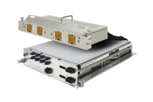
The T2000 ATE solution consists of a high-speed optical/electrical test module, a low-speed digital module for I2C ports, and a device power supply module (Figure 1), all of which are integrated into the test platform. The test module’s 64 ports can operate up to 28 Gigabits per second (Gbps). This includes 32 optical ports – 16 transmit (TX) and 16 receive (RX) – and 32 differential electrical ports (16 TX and 16 RX). The T2000 platform also includes high-performance device fixture technology for both the optical and electrical ports to perform device interface.
To understand the benefits the T2000 platform enables, let’s take a closer look at the device fixture and the high speed optical/electrical test module.
Device fixture and test module
The device fixture provides both optical and electrical signal connections between the device-under-test (DUT) and the test module. To test optical lanes, the device fixture must support such optical assemblies as MT-connectors. However, ordinary MT-connectors have a limited insertion lifetime (typically, less than 300 insertions), making them inappropriate for this application. To overcome this limitation, Advantest has developed a high-volume-capable non-contacting optical connector that is fully compatible with MT-connectors.
Figure 2 shows the new optical connector and illustrates the approach used for its fabrication. Using a gradient-index (GRIN) lens to maintain a working distance of 150 microns (µm) enabled development of a high-performance optical connection with no physical contact between the end of the fiber-optic cable and the connector. Because the new connector is MT-connector-compatible, it can be used to make contact with MPO connectors, which are typically used in compact QSFP+ PSM4 transceivers used for data communications.
The high-speed optical port block diagram is shown in Figure 3. FUNC ASIC has pattern generator (PG) and bit error rate tester (BERT) functionalities, both of which can operate up to 28 Gbps. For electrical ports, the FUNC ASIC is connected to the DUT via the device fixture. For optical ports, the output test signal from FUNC ASIC goes to the optical modulator to modulate the continuous wave laser provided by the laser source. Variable optical attenuators (VOAs) adjust output power to the DUT to test the DUT’s receiver sensitivity. The optical signal provided to the DUT is connected to a photo detector and trans-impedance amplifier (TIA) in the test module to convert it to an electrical 28-Gbps signal. Then FUNC ASIC captures the signal to measure eye diagram by using its BERT capability.
Measurement results
During device fixture evaluation, insertion loss variation was measured against iterations. The results, seen in Figure 4, showed stable insertion loss variation of less than +/-0.3 dB during 100,000 repeated operations. Compared to ordinary MT-connectors, which have an anticipated lifetime of less than 300 cycles, this connector can provide stable measurement with a longer lifecycle.
Current 100-Gbps datacom transceiver interfaces, such as PSM4, CLR4 or CWDM4, use four lanes of both optical and electrical 25-Gbps lanes to achieve aggregated band width of 100-Gbps. The test module has 16 lanes of both optical and electrical high speed ports. The scalable platform can simultaneously test four DUTs per optical port module; integrating two modules onto a test solution thus allows parallel test of up to eight DUTs. Multi-site testing increases system throughput and significantly drops per-site equipment costs.
Summary
The semiconductor industry roadmap for optical transceivers – advanced semiconductor devices that transmit and receive data through optical fibers – calls for boosting speeds from today’s 40-Gbps interconnections to as much as 400-Gbps by 2020. Advantest’s T2000 solution is among the first integrated solutions able to cost-efficiently test these high-speed devices.
Since typical 100G transceivers use four 25-Gbps ports to achieve aggregated bandwidth of 100-Gbps, the T2000 configuration allows four 100-Gbps devices to be tested simultaneously, improving test throughput and reducing system cost. It also includes a device fixture solution that provides stable and longer-lifecycle non-contacting optical connectors, making the system well suited for high-volume manufacturing environments.