This article is adapted with permission from Electronic Product Design & Test. The original article can be viewed here.
By Ira Leventhal, Vice President, Research & Venture, Advantest America, Inc.
As a consequence, test complexity is exploding for devices targeting AI server farms and data centers. Test complexity is increasing in part because process nodes are shrinking (more Moore). Additionally, complexity is rising because of heterogeneous 2D, 2.5D, and 3D integration (more than Moore). This integration increasingly includes CPO devices that replace high-power electrical I/O with lower-power optical communications.
Heterogeneous integration relies on advanced technologies like hybrid bonding and high-bandwidth memory stacking. These devices face challenges in high-speed data transfer, power, heat dissipation, and die handling. The power demand of electrical I/O can rival that of the processor core, pushing a shift toward optical data-communications using CPO devices. Additionally, testing in high-volume manufacturing requires tools for yield analytics and lifecycle data management, along with leading-edge test instrumentation, dynamic thermal control, and a robust data infrastructure.
Multiple test insertions
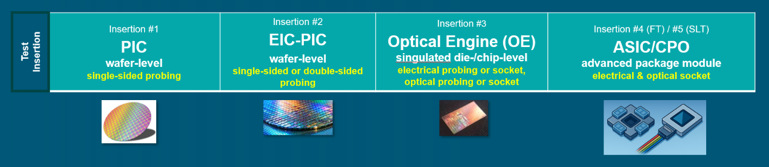
This increasing test complexity drives the need for fully automated, scalable tools for optical and electrical testing that can accommodate the five distinct test insertions required for CPO devices in HVM settings (Figure 1). Two of these insertions are at the wafer level. Insertion #1 provides single-sided photonic integrated circuit (PIC) wafer-level probing. After this insertion, the photonics wafer may be bonded to the electronics wafer, so insertion #2 provides single- or double-sided electronic IC (EIC) plus PIC wafer-level probing. Insertion #3 is the singulated-die/chip-level insertion of the optical engine (OE), requiring both electrical and optical probes or sockets, necessitating special die handling solutions. This step ensures that a faulty OE is not paired with a processor chip costing many thousands of dollars. The final two insertions require an electrical and optical socket to test the entire ASIC/CPO advanced package module; insertion #4 is a classical ATE final test (FT) of the packaged device, while insertion #5 is a system-level test (SLT) that mimics mission-mode operation.
All these insertions, which do not simply repeat the same tests, present significant challenges. Many successful test strategies aim to "shift left," or find defects as early as possible in the process. Success requires a cohesive ecosystem. No one industry player can solve the entire test complexity problem—it requires a deep level of collaboration across the ecosystem, from probe card vendors to instrument vendors.
Leveraging the installed electrical-test base
The semiconductor test industry lacks explicit standards for optical probing, optical-package fiber-connector handling, and optical instrumentation. As a result, test can require highly customized rack-and-stack instrumentation and time-consuming optical signal-path calibration. Work is proceeding, however, on fully automated, accurate, stable, and repeatable optical test solutions that leverage existing electrical test equipment. The ultimate goal is a highly integrated, standard, and fully scalable ATE with automated calibration and diagnostics that can fully test CPO devices at high throughput.
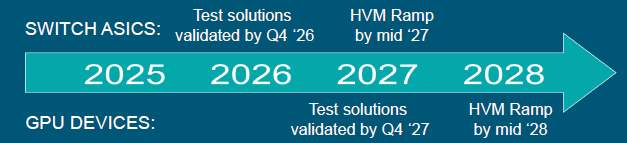
The need for CPO is now approaching a tipping point: some adoption of CPO is occurring at 200G/lane, and CPO will be mandatory at 400G/lane. Consequently, an industry roadmap is emerging for CPO FT/SLT test insertions in HVM (Figure 2). The roadmap shows that for switch ASICs, test solutions will be validated by Q4 2026, with HVM ramp-up beginning by mid-2027. For GPUs, each stage will follow one year later.
For both types of devices, HVM test strategies are focused on loopback approaches (for example, routing a transmitter output back to a receiver input) with the option of adding optical instruments. In addition, thermal control is necessary to keep optoelectronic devices within their mission-mode temperature range during test, keeping in mind that the optical engine will be located next to a processor operating at very high temperatures.
A sign of progress in the detachable connector landscape is that first-generation connector choices were made to move builds forward as the first step towards HVM. However, there may be a return to a "wild west" approach with multiple competing connector options as customers chase performance, leading to a mix of standard and custom solutions. Additionally, significant issues remain regarding hardened test connectors as well as their cleaning and servicing. And finally, many optical connectors are not built for test applications, and their performance can degrade in as few as 20 insertion cycles.
Aggressive ramp schedule
The aggressive HVM ramp schedule for CPO devices necessitates integrating optoelectronic test capabilities into existing manufacturing and test systems without extensive redesign. Equipment operators must build on their current setups rather than replace them. However, simply combining different benchtop setups in a "Frankenstein" approach won't meet the strict requirements for quality, reliability, scalability, and supportability needed for HVM testing. An effective HVM-ready test system requires intentional design focused on these stringent demands.
Several factors must be considered when implementing HVM solutions for CPO device package test. An HVM system should support multiple devices, enable fast changeover, integrate automated cleaning, and maximize throughput and uptime while limiting mechanical complexity.
New key requirements for optical components include using hardened optical test connectors, maintaining polarization on the external laser source (ELS) output, and minimizing losses. Polarization drift that occurs in the continuous wave output of the external laser source (ELS), which essentially serves as an optical power supply, can compromise the performance of the modulators in the DUT's OEs. While DSP-based error correction approaches are highly effective on modulated signals, they cannot be applied pre-modulation, so great care must be taken to provide a clean ELS input to the OEs. Important steps to follow include:
- Using polarization-maintaining optical fiber (PMF).
- Minimizing the number of connectors in the optical path, because all connectors contribute to increased insertion loss and polarization loss, as well as reduced polarization extinction ratio (PER).
- Ensuring all connectors are precisely aligned and polished to optimize PER.
- Establishing an ongoing calibration and verification process to regularly check that the optical signal path meets spec.
Modular platform approach
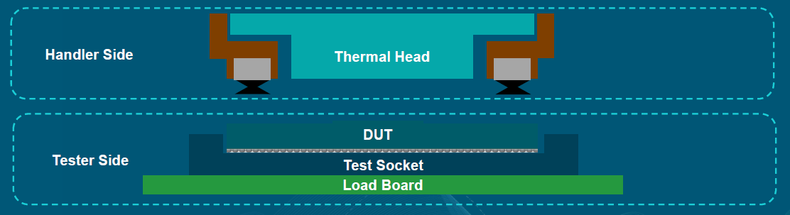
Advantest's platform approach to high-performance compute (HPC) and AI device testing is based on a split architecture that cleanly separates the tester and handler sides of the system (Figure 3). This architecture allows each element—thermal head, mechanical handling, test socket, load board, and DUT interface—to operate within a structured framework optimized for performance and scalability. By decoupling these layers, the system ensures stable thermal management, improved mechanical reliability, and consistent electrical performance under the extreme requirements of current and future HPC and AI devices.
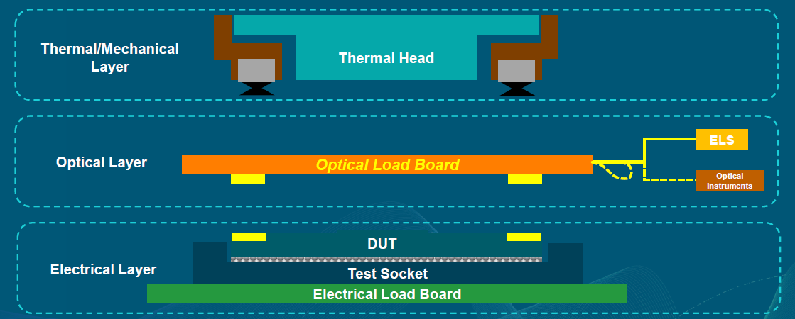
With CPO entering the picture, this architecture is refactored into multiple specialized layers, each responsible for a distinct function (Figure 4). An Optical Layer is added, centered around an Optical Load Board that provides reliable, repeatable contact to the CPO connectors and smooth integration of the ELS inputs and optical instrumentation. This layer is integrated between the traditional electrical and thermal/mechanical layers to form a cohesive test solution tailored for CPO devices. This layered approach enables advanced optical capabilities without forcing a disruptive redesign of the entire test cell. In essence, optical capability becomes a natural extension, not a structural overhaul.
This platform-based approach delivers substantial advantages for scaling into high-volume manufacturing (HVM). Its modular architecture enables a seamless progression from NPI to high-throughput production, while built-in automation improves operational efficiency and reduces operator burden. Because it remains fully compatible with the installed base—testers, handlers, load boards, and sockets—customers can introduce CPO capability without retooling their factories. At the same time, the platform's flexibility accommodates both switch ASICs and GPUs, multiple connector formats, and parallel test configurations, broadening coverage across diverse CPO device families.
Equally important is the system's versatility in test strategy. Whether the workflow relies on optical instrumentation, loopback-based validation, or a hybrid approach, the same platform supports each method within a unified hardware and software environment. This consistency enables optimized test flows across insertions and simplifies operational management. The result is a high-uptime, high-throughput solution engineered for performance and reliability: hardened optical connectors, automated cleaning, rapid changeover fixtures, and automated calibration processes all work together to maximize overall equipment effectiveness (OEE).
Conclusion
A platform-based approach for CPO HVM test emphasizes intentional design, ensuring cohesive, robust solutions instead of improvised, ad hoc ones. Such an approach is critical for success in CPO test in the Era of Complexity, driven by the emergence of CPO devices in the HPC/AI environment, and it ensures scalability, automation, and compatibility from NPI to HVM. Advantest is leveraging its in-house expertise and working with key ecosystem partners, including leading prober and probe card vendors as well as connector and instrument vendors, to ensure the aggressive rollout of CPO-ready HVM test solutions.