Editor's note: This article is adapted from a February 11, 2026, SEMICON Korea presentation titled "Evolving Test Distribution in the Age of AI."
By Fabio Pizza, Business Segment Manager, Advantest Europe
The proliferation of artificial intelligence (AI) is driving rapid acceleration of the semiconductor market, which analysts now predict will reach $1 trillion this year. Many semiconductor devices will be the GPUs that populate the data centers that run AI workloads. Driven by strong, sustained investments from hyperscaler operators, high-performance computing (HPC)/AI data centers are expected to account for a large portion of the market. This market is driven by the growing demand for computational capability, with training computing requirements for generative AI models having increased fourfold each year since 2018 in terms of floating-point operations per second (FLOPS). In addition, semiconductors will also find increasing use in consumer-facing AI-related products such as AI-enabled PCs, smartphones, artificial-reality systems, autonomous taxis, and humanoid robots.
As the market expands, the semiconductor devices themselves are evolving. Moore's Law is making less of a contribution to successive process generations as it reaches fundamental physical limits, so chip designers are turning to More than Moore—they are building larger 3D packages with more chiplets and accelerator cores, as well as voltage regulators and passive devices integrated within the substrate to bring power delivery as close as possible to the individual processors being powered. And because latency and throughput bottlenecks can limit cluster performance, designers are increasing high-bandwidth memory (HBM) capacity and are boosting chip-to-chip bandwidth with co-packaged optical (CPO) and high-speed electrical interfaces.
Accelerated test challenges
The growing complexity of AI-focused semiconductor devices presents major challenges for semiconductor test operations. Transistor counts continue to rise steeply, leading to a corresponding increase in structural and functional test content.
Power has emerged as one of the most critical constraints in test environments. Device power requirements are increasing rapidly, requiring automated-test-equipment (ATE) to deliver very high currents with precise regulation and measurement accuracy. High-power device power supplies must scale flexibly, support ganging, and maintain consistent performance under dynamic loads. These higher power levels also necessitate more advanced protection mechanisms and more detailed voltage and current profiling to ensure device safety and test interface contact integrity.
Thermal management is becoming equally critical. As test power levels rise into the multikilowatt range, active thermal control (ATC) is increasingly required, at wafer, die-level and package test levels. Effective thermal management demands real-time monitoring of power consumption and temperature, along with predictive AI capabilities that can anticipate thermal excursions and respond proactively.
Packaging trends compound these challenges. Advanced 3D packages and multi-chiplet assemblies continue to grow in size, making device handling and multisite testing more difficult. Larger sockets consume more space on test boards, increasing the complexity of connecting ATE resources. Finally, the appearance of optical capabilities necessitates the adoption of integrated electro-optical test solutions, requiring the deployment of optical instrumentation at the wafer-probe through final-test stages.
Accelerated test-engineering effort
Deploying the necessary test resources while speeding time to market for complex devices will require an accelerated test-engineering effort. That effort will require chiplet support with the concurrent test of heterogeneous and homogeneous cores on the same substrate. In addition, test encryption will be required to protect IP in multivendor environments. AI will have a key role to play in code generation and debugging, as well as in allowing the merging of test flows to increase test parallelism and reduce test time.
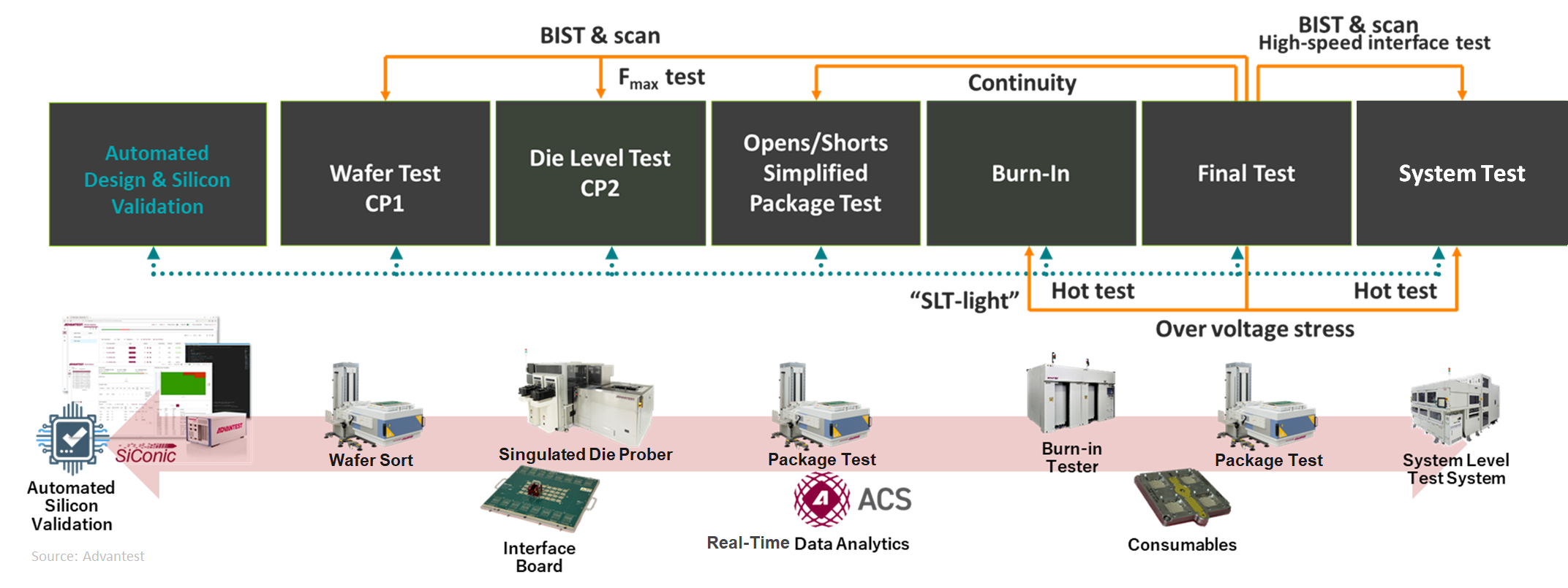
The increase in complexity will continue to drive the test workflow. By the end of the decade, GPUs will have 1 trillion transistors each, and AI clusters will include 1 million GPUs. Because test content scales with transistor count, test must meet ever stricter defective part-per-million (DPPM) requirements. The production-test process will require multiple insertions, extending from die-level testing to burn-in and system-level test (SLT), along with optical test. Preventing total test times from becoming prohibitively long will require optimized test insertions to reduce cost of test (COT) and speed time to market (TTM), and it will become critical that test content be executed at the proper insertion step, which can be facilitated through seamless test-content portability that enables the movement of tests from one insertion to another. The result is an efficient test distribution that optimizes DPPM, TTM, and COT.
Test content on the move
In the age of complexity, test content is on the move, with the goal of optimizing test distribution to meet quality goals. Early-stage test focuses on identifying known good die and enabling intelligent assembly of multi-die packages, minimizing material waste and avoiding the cost of packaging defective components. Later-stage test focuses on ensuring system-level reliability and detecting defects that only appear under real-world operating conditions. Figure 1 shows an overview of this process, extending from validation through system-level test.
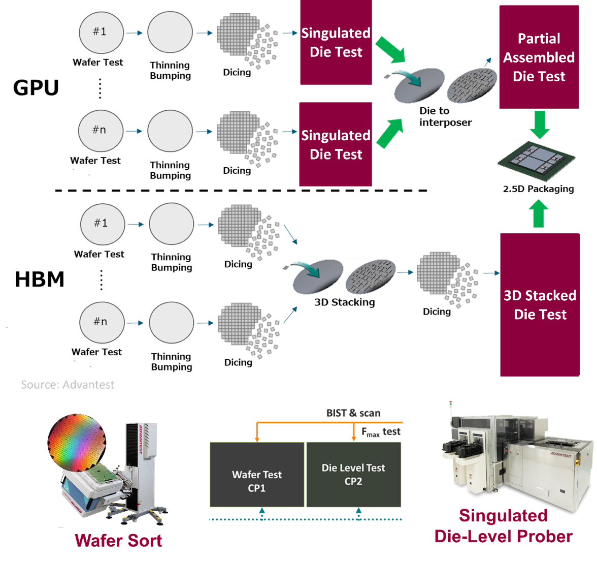
Shifting left, as illustrated in Figure 2, can increase yield. With HBM and CoWoS packaging contributing about 70% of the total cost, it becomes critical to shift content left to the wafer and die level to identify known good die and perform die matching, ensuring that good parts are packaged only with other matched good parts in 2.5D/3D packages, thereby reducing cost and material waste. Thermal control and system-like test scenarios are also increasingly applied at earlier stages.
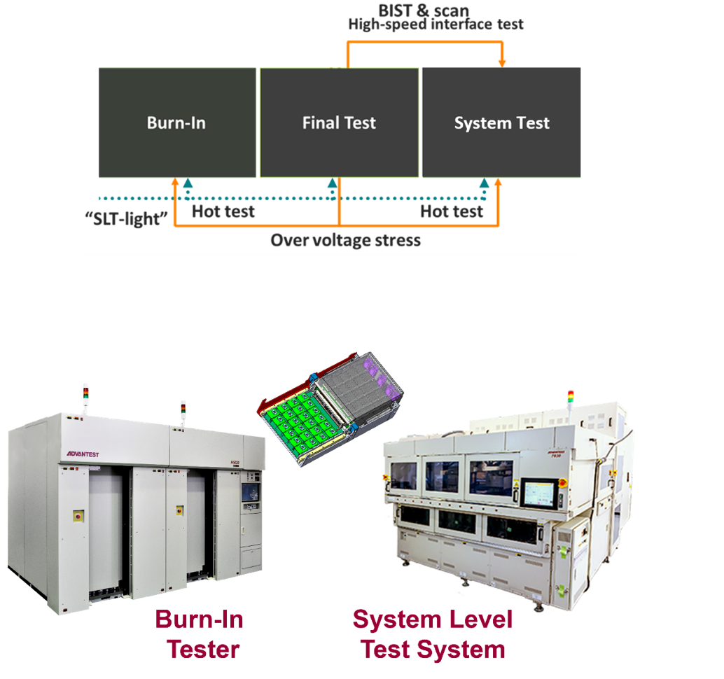
Shifting right to execute tests after packaging, as shown in Figure 3, increases test quality by driving DPPM down before product shipment. System-level test environments can expose defects related to software interaction, timing variability, and thermal stress that are not visible at lower levels of testing. While such tests can be time-consuming, high-parallelism strategies help mitigate their impact on throughput.
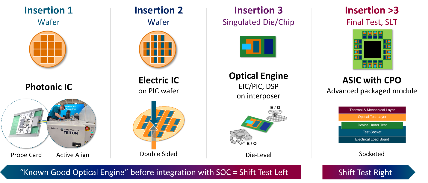
Optical integration, as shown in Figure 4, introduces additional insertions into the test flow, including photonic device test and combined electronic-photonic module verification. Also in these cases, test content must shift both left and right to ensure that individual components and integrated subsystems meet quality and performance requirements before final assembly.
Conclusion
The era of AI complexity is redefining test-distribution strategies to accommodate skyrocketing test content requirements. Effective test requires high volumes of test data along with the means to analyze that data and make real-time decisions across the test floor. In addition, test now requires high power levels and ATC across all test insertions.
To effectively meet these requirements, ATE is evolving from a pure defect-detection system to one that provides system-level validation supported by AI software tools. Optimal test distribution for meeting quality, TTM, and COT goals requires strong collaboration among technology partners across the semiconductor ecosystem.