


TS9000
Growing global adoption of smartphones and tablets with thin form factors is driving demand for semiconductor devices to be smaller and more highly integrated. Extremely precise mold thickness management is necessary for these cutting-edge semiconductor processes. However, quality management in the molding process has been challenged by the fact that non-destructive mold thickness measurement tools were not available, meaning that engineers must extract individual device samples during the trim and form process, cut them destructively, and inspect the cross sections by microscope. This is a time-consuming process typically involving a long wait time due to a bottlenecked queue.
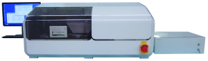 Advantest’s TS9000 Mold Thickness Analysis (MTA) System solves these issues by utilizing terahertz waves to measure mold thickness non-destructively, rapidly, and with a high degree of precision. The system’s high throughput enables users to test large volumes of samples and readily grasp the mold thickness distribution of entire lots. For the first time, users can inspect mold thickness during volume production.
The TS9000 works by placing the semiconductor devices to be measured on the measurement unit’s XY stage. It rapidly evaluates multiple “measurement points” and analyzes the mold thickness distribution. By re-using files containing sets of measurement points (“recipes”), the system can easily inspect devices of the same type without reprogramming. During measurement, it can display thickness measurements and reflection waveforms from each measurement point in real time. These data are recorded in files for each production lot, and can be used for online data management.
The system overcomes the limitations of traditional measurement methods by enabling repeatable and highly accurate measurements, even when analyzing the optically opaque mold polymer materials typically employed in circuit packages. It can handle die in strips or singulated units and is also fully compatible with industry-standard JEDEC trays. During testing, the display shows the status of samples being analyzed along with other important information, allowing the operator to fully monitor test progress.
Fully non-contact and non-destructive, the TS9000 can be configured for partial or 100-percent inspection of the product. Analysis points are fully user defined, ranging from one to 20 points per unit. In addition, the system is fully adaptable for use at various points in the assembly and packaging process, including earlier stages where it can improve product quality and yield.
For more information, please email THz_info@advantest.com or visit Advantest.com.