Pages Menu
TwitterRSSFacebook
Categories Menu

Posted in Top Stories

Rethinking Security in Semiconductor Testing: Why Containment Is the New Imperative

This article is adapted with permission from a recent Advantest blog post.

By Arik Peltz, Director, Technical Product Marketing, Advantest Cloud Solutions (ACS)

It’s nearly impossible to keep up with the headlines without stumbling upon another major cybersecurity incident. According to recent reports, 2024 witnessed a staggering 5.5 billion breaches globally. In the United States alone, the average cost of a single data breach clocked in at $9.36 million—slightly lower than 2023’s figure, but still a significant hit for any organization. On a global scale, the average breach cost was $4.88 million, reinforcing that the threat landscape is both vast and expensive.

Perimeter defenses are no longer enough

Traditionally, cybersecurity in semiconductor manufacturing and test environments has centered around perimeter defense—blocking threats before they enter. These measures include timely software updates, closing unused network ports, deploying firewalls, running IDS/IPS tools, and enforcing strict password protocols. While foundational, these practices fall short in the face of today’s diverse and evolving threats.

Why? Because the scope of potential vulnerabilities continues to grow. It’s not just about outdated software anymore. Misconfigured devices, overlooked network components, and even human error—like someone plugging in an unknown USB drive—can expose a facility. It’s clear: breaches are no longer rare events. They are inevitable. The challenge now lies in what happens after a breach occurs.

The semiconductor test floor: complex and exposed

A semiconductor test facility is far more intricate than it might appear. The test cell may be the focal point, but it operates within a larger network of systems—ranging from HVAC units and network switches to printers and third-party software tools. These are all potential gateways for exploitation.

Further complicating matters is the need for seamless cloud connectivity. Many test operations rely on real-time data sharing with external stakeholders for performance analytics and optimization. That constant network exposure, while essential for business operations, makes the environment even more susceptible to attacks.

The evolving nature of cyber threats

Today’s cyberattacks are smarter, stealthier, and increasingly driven by artificial intelligence (AI). Many use social engineering to build trust and then employ malware that mimics normal system behavior. These “slow burn” attacks can run undetected for extended periods, slowly extracting data or altering system operations. Conventional security systems often can’t spot these subtle anomalies in time.

The rise in customer-facing data sharing exacerbates this issue. As test facilities transmit more data to clients, they inadvertently widen their attack surface. Without a robust containment strategy, these vulnerabilities can become entry points for more sophisticated breaches.

Introducing a containment-first approach: True Zero Trust™

To address these challenges, Advantest advocates for a containment-first strategy, embodied in its True Zero Trust™ Environment. This model borrows its philosophy from high-risk environments like the International Space Station, where systems are designed to automatically isolate compromised sections to prevent broader damage.

Here’s how it works:

  • Automated containment gates on the test floor that activate in response to suspicious activity
  • Built-in assumption that threats can move both upward and downward across the facility
  • Shared accountability between OSATs and fabless companies for maintaining a secure test floor
  • Full traffic visibility via packet inspection and detailed logging
  • Encrypted communications between equipment and central containment servers
  • Verification of third-party software through mandatory software bills of materials (SBOMs)

This model doesn’t just focus on keeping threats out—it plans for when, not if, they get in. Every node, transaction, and data packet is treated as untrusted until proven otherwise.

The power of ACS RTDI™

At the heart of Advantest’s containment strategy is the ACS Real-Time Data Infrastructure (ACS RTDI™). This platform provides the foundation for building a secure, flexible, and data-rich test environment.

ACS RTDI™ includes:

  • A communication backplane spanning the entire test floor
  • Edge computing nodes that allow local processing and reduce data exposure
  • Advantest Unified Server for orchestration and policy enforcement
  • A containerized application hub that supports isolated, scalable software deployment

ACS RTDI™ not only facilitates secure operations but also unlocks advanced capabilities such as adaptive test, data feedforward and backward, outlier detection, and AI-driven predictive modeling. It’s security and innovation, rolled into one powerful solution. 

Looking Ahead: Secure Innovation as a Competitive Edge

The future of semiconductor testing is moving toward intelligent, semi-autonomous systems powered by AI. These applications demand real-time responsiveness and uninterrupted data flow—both of which are incompatible with outdated security models.

Containment isn’t just a cybersecurity necessity—it’s a foundation for innovation. Through the True Zero Trust™ framework and ACS RTDI™, organizations can safeguard their intellectual property while enabling breakthrough performance enhancements.

To further support this vision, Advantest offers the ACS Solution Store—a digital marketplace featuring software modules tailored to AI/ML, big data analytics, and secure test operations. These tools are designed to be customizable, scalable, and ready to meet the evolving demands of the semiconductor industry.

Read More

Posted in Top Stories

How AI Enables Adaptive Probe Cleaning

This article is adapted with permission from Electronics360. The original article can be viewed here.

By Nunzio Renzella, Specialist System Engineer, Advantest Europe GmbH

Test cost reduction is a key goal of semiconductor ATE customers, with major cost factors being test time, the test cell, and—for wafer-probing process—the probe card. Maintaining probe card cleanliness is a key aspect of a successful test process. Lack of cleanliness can result in good devices being rejected, but frequent probe card cleaning is time-consuming and increases the cost of test.

To optimize the cleaning interval, a new technique called adaptive probe card cleaning (APC) employs artificial intelligence (AI) and machine learning (ML) to provide real-time monitoring of probe card performance, initiating probe card cleaning only when necessary. The technique improves test efficiency and extends probe card life, resulting in cost savings and consistent performance while providing valuable insights that provide a competitive advantage.

Probe card cost breakdown

Probe card costs include the original purchase price. Probe cards are generally considered consumable products that need to be replaced, but during their useful life, they also incur online and offline maintenance costs. Online maintenance is performed inside the probe station, while offline maintenance requires the removal of the probe card for needle adjustment and replacement, tasks usually performed by the probe-card manufacturer.

In addition, probe cards incur costs related to the cleaning sheets required for the online cleaning process. One estimate puts the initial probe card purchase cost at 40% of the total probe card cost, with maintenance accounting for 55% of the total cost and cleaning sheets adding another 5%.

These figures point to maintenance cost as a key target for overall probe card cost reduction, and online maintenance costs are greatly influenced by the cleaning frequency. Currently, as illustrated in Figure 1, probe cleaning occurs on a fixed cleaning cycle based on a tradeoff between cleaning costs and yield loss. Complicating the estimation of the optimum cleaning cycle is the fact that yield loss varies from product to product and lot to lot. In the figure, for example, probing yield loss degrades much more quickly for lot B than for lot A. Taking into account cleaning costs and the wide range of yield losses, the customer in this example has estimated, based on practical experience and experimentation, that the “best” cleaning interval is at the 100-shot point.


Figure 1. Customers trade off cleaning costs (red trace) against yield losses (black traces) to determine the “best” cleaning interval (green bar).

Shifting the cleaning interval

In an effort to better optimize the timing of the cleaning cycle, Advantest has developed the software-based APC technique that applies AI algorithms to assess the condition of the probe needles in real time and to perform cleaning only when dirty needles begin affecting yield. In the Figure 2 example, APC enables probe cleaning to shift right to the 200-shot point, providing significant cost savings. 

Figure 2. APC can allow cleaning to be shifted to the right (to the yellow bar), saving overall cleaning time and costs.

The APC AI algorithm functions by observing failure trends among different sites. If trends differ between two sites, the algorithm judges that one or more needles are dirty on the site exhibiting the most failures, and it sends a general-purpose interface bus (GPIB) command to the prober to initiate the online cleaning cycle.

Figure 3 provides more detail on how to determine if the needle tips are dirty. For case 1 on top, the failure balance has significantly broken down, with site 1 showing many more failures than site 2. Consequently, the APC algorithm judges that a cleaning is required for site 1. For case 2 on the bottom, the failure balance remains relatively constant, and APC judges that cleaning is unnecessary; the observed failures may result from a wafer production issue. 

Figure 3. For case 1, the failure rate is out of balance, indicating a need for cleaning, while the relative balance of case 2 indicates that cleaning is not necessary.

A potential issue with APC arises when a continuous failure at a specific site results in APC triggering too many cleaning actions. To prevent this situation, APC can observe whether a cleaning has resolved an issue. If not, it concludes that the issue has a root cause other than a dirty needle, and it activates an Auto Bin Disabling function, which disables monitoring of the problematic site and bin. The customer can choose whether or not to use this function.

APC flow

The APC implementation flow (Figure 4) begins with a learning phase with a pre-fixed cleaning cycle (equal to the cycle used by the customer in the conventional probing approach) for the first wafer in a lot. The APC AI algorithm employs ML to determine the pass/fail tendency of each site. If the ML from the first wafer is successful, the adaptive-cleaning phase begins with the second wafer and continues with subsequent wafers, with cleaning performed whenever contamination is detected. If the ML is not successful on the first wafer due to low yield, the learning phase continues with the second wafer.


Figure 4. An AI algorithm employs ML on the first wafer and applies APC to other wafers in a lot.

Tester and prober independent

APC is adaptable and flexible. It works with Advantest’s T2000, V93000, and T6000 SoC test systems, as well as with other companies’ ATE systems. It also works with a variety of probers, including those from Accretech, SEMICS, and TEL, and with a variety of cantilever, vertical, and other probe-card types. APC supports parallel counts from two to 256 sites.

In addition, the APC algorithm executes in less than 1 ms per shot and will have a negligible impact on test throughput. Customers do not need to modify their test programs, and APC can run on the tester controller, so they do not need to add any specific hardware. Also, APC does not require access to Standard Test Data Format (STDF) data or any specific parametric data. Customers can use a standard prober driver, but they will need to add a GPIB command for initiating the cleaning process, and they will need to modify the prober recipe by adjusting the prober parameter setting.

Figure 5 summarizes the differences between the traditional fixed cleaning cycle (top) and the APC cycle (bottom), with the horizontal axis showing the elapsed time. As shown for the fixed cleaning cycle, a probe can become contaminated well before the 100-shot fixed cleaning interval, potentially resulting in many good devices being rejected (during the times indicated by the solid red arrows).


Figure 5. Fixed-cycle cleaning (top) can result in the rejection of good parts, while APC (bottom) can save these devices.

However, APC can detect contamination in real time, minimizing yield loss due to dirty needles and saving devices tested during the time indicated by the outlined red arrows.

APC results

APC has yielded favorable production line results. Based on one year of data, one customer reported that on one fab testing 37,000 wafers, it saw a 75% average cleaning reduction, and on another fab testing 10,000 wafers, it found a 50% to 80% reduction, both while maintaining the same yields. The same customer reported that probe card lifetimes were extended by 35% to 100%.

A second customer, using four different vertical probe card types, reported an online cleaning reduction of 65%, a yield improvement of 0.6%, and a lot test-time reduction of 7.4%. This customer also found that probe card life doubled and probe card maintenance costs were reduced by 50% per year.

To illustrate how APC can help prospective customers, Advantest offers an APC offline simulation capability. These customers can send Advantest STDF files for several wafer lots as well as information on the current probe-cleaning interval setting. Advantest will return an APC simulation report stating the achievable cleaning reduction ratio and including HBIN sequencing maps showing when and where the cleaning occurred.

Conclusion

Several factors can lead to probe tips becoming dirty, but many are unpredictable, and test managers must expect that the probe tips can become dirty at any time. APC can determine when this condition occurs, and it can take the appropriate cleaning action at the appropriate time. 

APC offers several specific benefits. It prolongs the life of probe needles, reduces probe-card maintenance costs, reduces yield loss, and shortens lot inspection times. In addition, customers need not manually adjust the cleaning cycle in response to new observations, and the optional Auto Bin Disabling function can automatically avoid continuous failures. Finally, APC reduces test time by eliminating extraneous probe-card cleaning and realignment after cleaning. 

Read More

Posted in Top Stories

AI Memory: Enabling the Next Era of High-Performance Computing

By Tadashi Oda, Senior Director of Memory and System Engineering, Advantest America

The rapid advancement of artificial intelligence (AI) is driving unprecedented demand for high-performance memory solutions. According to TechInsights, AI-driven applications are fueling a 70% year-over-year growth in high-bandwidth memory (HBM). However, as AI models grow in complexity—from large language models (LLMs) to real-time inference applications—the need for faster, higher-bandwidth, and energy-efficient memory architectures has become critical.

HBM devices consist of multiple stacked DRAM chips. The reduced mounting area and heightened wiring density of the stacked structure improve speed, capacity, and power consumption. Memory-intensive applications, such as high-performance computing (HPC), graphics processing units (GPUs), and AI accelerators, areas once dominated by DDR and GDDR memory, rely on HBM to meet the data throughput requirements of training and inference. At the same time, power-efficient alternatives such as low-power double data rate (LPDDR) are gaining traction in AI servers, where energy consumption is a primary concern. These trends, alongside the increasing integration of AI in mobile and edge applications, are shaping the future of AI memory technologies. However, these advancements bring significant test and validation challenges, requiring innovative solutions to ensure performance, reliability, and cost efficiency.

Market evolution and growth drivers

AI has become the dominant driver of innovation in the semiconductor industry, creating unprecedented demand for memory technologies. The computational complexity of AI models—particularly large language models and generative AI applications—has pushed GPUs and AI accelerators to their limits, requiring memory solutions that can sustain high-speed data access and processing; see Figure 1. HBM has emerged as the preferred solution for AI training workloads, offering multi-die stacking architectures that significantly increase memory bandwidth while minimizing power consumption.

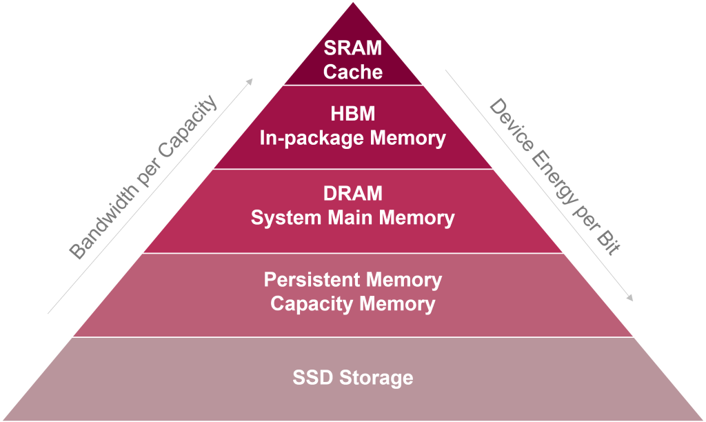
Figure 1. AI data: near-memory compute for energy-efficient systems.

Beyond training, AI inference workloads are expanding into new applications, including mobile devices, automotive systems, and consumer electronics. These deployments require memory solutions optimized for efficiency, low power consumption, and cost-effectiveness. LPDDR, originally designed for mobile applications, is now gaining traction in AI servers due to its ability to deliver high performance with reduced power usage. As AI continues to move from centralized data centers to distributed computing environments, the demand for diverse memory architectures will continue to grow.

Investment in AI infrastructure is accelerating, with hyperscale data centers expanding their AI server capacity to accommodate increasingly complex models. AI workloads require not only high-performance memory but also specialized storage solutions that can handle vast datasets efficiently. The expansion of inference applications beyond data centers is also reshaping memory demand, as AI capabilities are integrated into smartphones, autonomous vehicles, and edge computing devices.

While AI-related markets are seeing rapid growth, traditional memory markets—including automotive, PCs, and mainstream mobile devices—are experiencing soft expansion. This shift reflects the broader industry transition from general-purpose computing to AI-driven architectures. As more AI workloads transition from training to inference, the balance of memory demand will continue to evolve.

AI memory architectures rely on advanced packaging techniques to optimize performance and power efficiency. The adoption of 2.5D / 3D stacking, heterogeneous integration, and silicon interposers enables higher memory densities and faster communication between memory and processors, as shown in Figure 2. These innovations improve AI system performance but introduce new challenges in manufacturing, validation, and test.

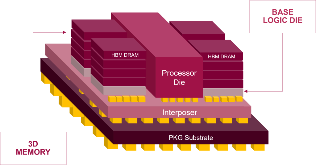
Figure 2. A diagram showing a typical HBM DRAM stack.

Ecosystem collaboration is also essential to advancing memory packaging technologies. Memory vendors, semiconductor foundries, and AI chip manufacturers must work closely to ensure seamless integration of next-generation memory architectures. Multi-die stacking and interposer-based designs require sophisticated testing and validation processes to detect defects early and optimize yield. As AI-driven memory solutions become more complex, new test methodologies will be required to ensure reliability and scalability.

The AI memory supply chain is undergoing a significant transformation, with increased vertical integration among semiconductor companies. Leading foundries are expanding their role in memory packaging and testing, consolidating manufacturing processes to improve efficiency. This shift requires closer collaboration between memory suppliers, GPU manufacturers, and semiconductor fabs to optimize design and production workflows.

At the same time, supply chain constraints—particularly in high-performance silicon interposers and through-silicon via (TSV) technologies—are impacting memory production. AI-driven demand for HBM and LPDDR is straining existing manufacturing capacity, making supply chain coordination more critical than ever. Companies must navigate these challenges while maintaining production efficiency and meeting the growing needs of AI applications.

Technology advancements in AI memory

HBM has become the foundation of AI computing, evolving from traditional DDR and GDDR memories to multi-die stacking architectures that deliver extreme bandwidth and low latency. Figure 3 depicts this evolution. The ability to stack multiple memory dies vertically and integrate them with high-speed interconnects allows AI accelerators to process massive datasets more efficiently. However, these advanced designs present unique challenges in manufacturing and test.

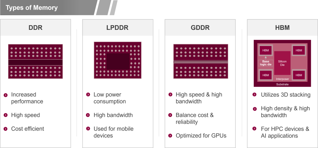
Figure 3. Descriptions of commonly used types of memory devices.

As AI workloads expand beyond data centers, power efficiency is becoming a key consideration in memory design. LPDDR, originally developed for mobile devices, is now being adopted in AI servers to reduce power consumption while maintaining high performance. Although LPDDR carries a higher upfront cost than traditional DDR memory, its long-term energy savings make it an attractive option for large-scale AI deployments.

Balancing performance, cost, and power efficiency is a major challenge for AI memory architects. LPDDR must be rigorously tested to ensure it meets the performance demands of AI applications while maintaining the power-saving benefits that make it viable. As AI adoption grows in power-sensitive environments such as mobile and edge computing, LPDDR is expected to play an increasingly important role in AI memory solutions.

AI workloads require specialized storage solutions that can handle the massive data volumes associated with model training and inference. Enterprise AI storage relies on high-speed solid-state drives (SSDs) designed to support AI-driven workloads, enabling fast data retrieval and processing in hyperscale data centers. Meanwhile, edge and on-device AI applications depend on Universal Flash Storage (UFS), a high-speed, low-power interface optimized for flash memory in mobile devices.

Ensuring the performance and reliability of AI storage solutions requires advanced testing methodologies. Both enterprise SSDs and mobile UFS solutions must be validated under AI-specific workloads to ensure they can handle the demands of real-time AI processing. As AI applications continue to diversify, memory and storage technologies will need to evolve accordingly.

Another AI memory function advancement is processing-in-memory (PIM) technology. AI training and inference require significant computational or mathematical resources to operate a combination of matrix multiplications, vector operations, activation functions, or gradient calculations. Figure 4 illustrates the benefits of implementing PIM in conjunction with LPDDR.

The purpose of PIM is to implement processing features inside the memory chip to reduce data movement between the memory and the processor. Because it reduces power consumption and increases performance, PIM is considered particularly effective in the mobile space for enabling a range of AI-powered applications. PIM is one example of how semiconductor memory is a critical component for the AI industry and illustrates how technology continues to evolve to advance future AI capabilities.

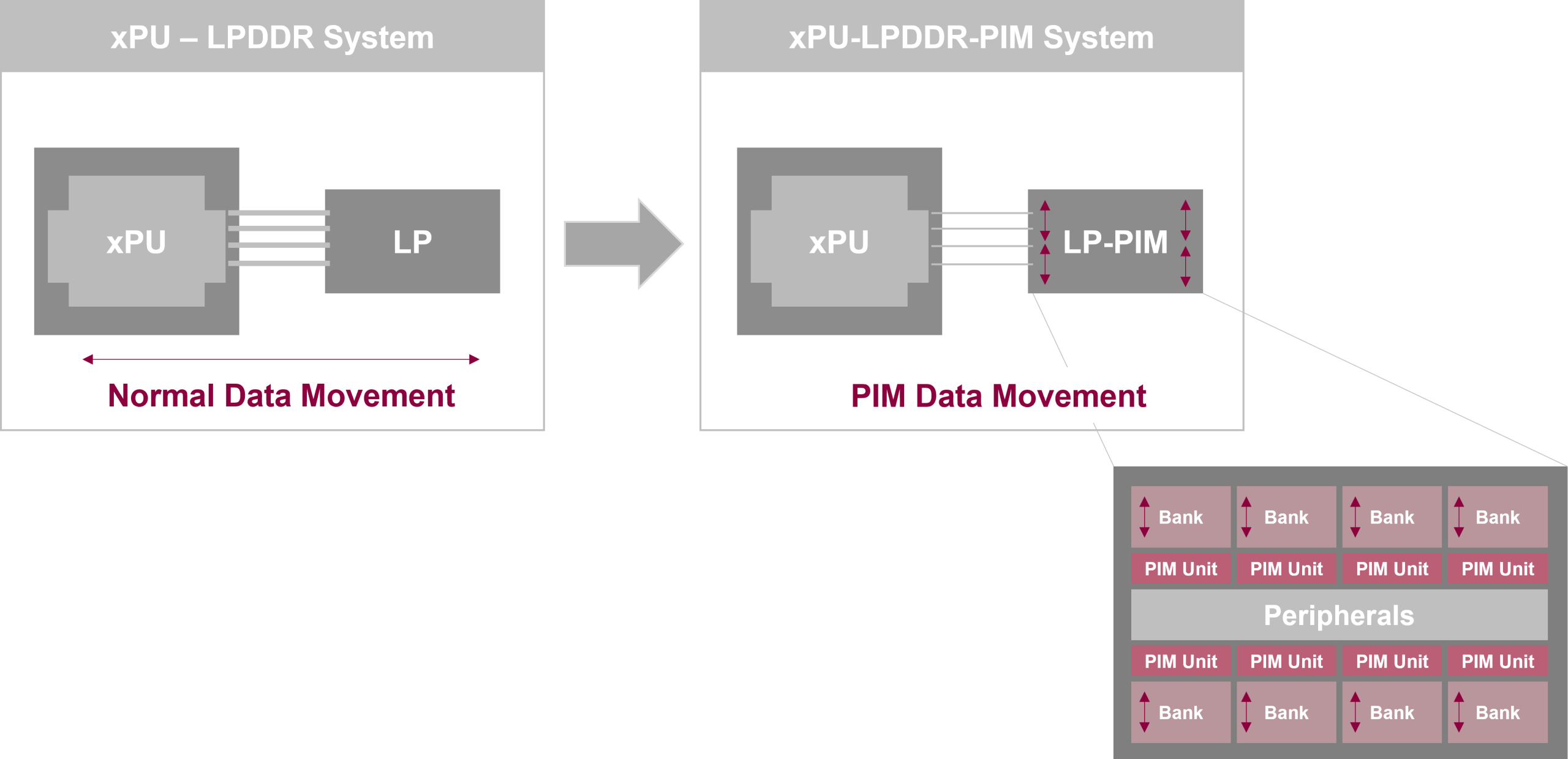
Figure 4. Memory in the AI/ML and data era.

Key market and test challenges for HBM

Ensuring the reliability of HBM stacks requires multiple test insertions throughout the production process. Each die within the stack must be validated for performance and integrity before final assembly, as shown in Figure 5. Before stacking, manufacturers perform wafer test that consists of burn-in stress, trimming, failure analysis and repair processes to ensure all memory cells work properly. The logic base die is also tested at wafer-level through SCAN test, IEEE1500 test, and logic test. Additional tests are performed after the DRAM die are stacked on top of the logic base die wafer, including burn-in stress test, DRAM array test, logic die test and high-speed operation test to ensure proper TSV connectivity within the DRAM stack. Advantest has been collaborating with DRAM vendors to develop HBM tests since before volume production began. As a result, the company now supports all test processes essential for the mass production of AI devices.

Thermal management is also a critical consideration, as the increased power density of HBM configurations can lead to overheating and performance degradation. As AI workloads continue to push memory technology forward, new innovations in stacked memory design and thermal control will be essential. Relating to thermal management, the high-power consumption of AI memory solutions is also a concern. Enhanced thermal control solutions, including precision cooling mechanisms, are necessary to address heat dissipation challenges. 

Increasing AI memory complexity heightens the challenges associated with the testing and handling of these devices. Ensuring die integrity during stacking and transportation requires the development of specialized die carriers to mitigate physical damage. Advances in automated handling systems improve secure stacking and assembly, reducing manufacturing defects.

The memory supply chain is also evolving, with vendors collaborating more closely with fabs and GPU manufacturers. The shift from siloed production models to integrated development ecosystems aims to overcome supply constraints and streamline production. However, challenges remain, particularly in securing high-performance silicon interposers and TSV technologies, which are essential for advanced memory integration.

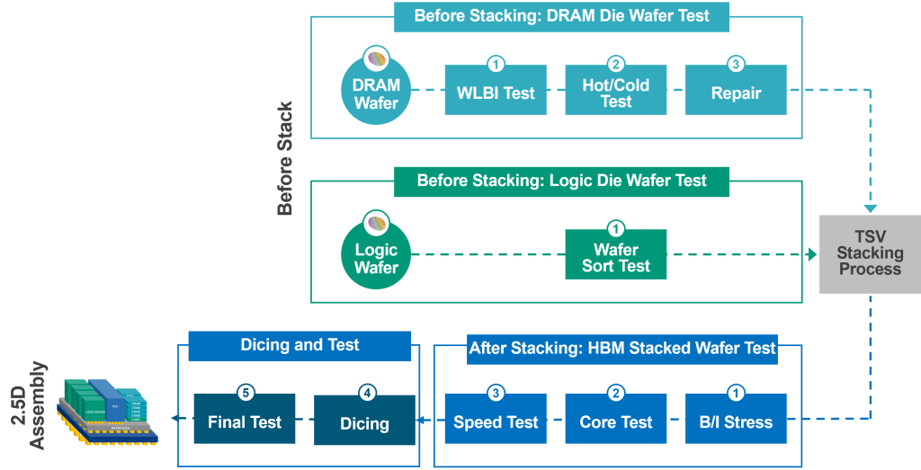
Figure 5. Test and assembly process for advanced memory devices.

Advantest’s solutions and market leadership

Advantest is at the forefront of AI memory testing, offering comprehensive solutions that address industry challenges. Various products in the company’s T5000 series, such as the T5833, provide high-speed, high-accuracy testing for HBM configurations, incorporating multi-step validation processes to ensure die integrity. Its modular architecture provides flexibility to scale with evolving test requirements, optimizing cost and efficiency for high-throughput production environments. This means that the platform is prepared for future testing of LPDDR6 devices as well as mobile storage protocols like UFS. 

Moving forward in this space, HBM4/E increases power consumption, doubling the DQ pin count in the DDR bus to 2048 DQs. The industry is also considering the development of “custom HBM” to tune specific areas of the AI workload. Advantest is working with industry-leading GPU and ASIC companies and hyperscalers to prepare for custom HBM testing.

Advantest’s proprietary die carriers ensure secure handling, minimizing physical stress on stacked memory dies and preventing defects during high-volume production. The company recognizes the need for handlers that provide superior thermal capabilities to address the growing demand for precision temperature management in AI memory applications.

The latest addition to the T5000 series, the T5801 ultra high-speed memory tester, is engineered to support the latest advancements in high-speed memory technologies —including GDDR7, LPDDR6, and DDR6— critical to meeting the growing demands of AI, HPC, and edge applications. Featuring an innovative front-end unit (FEU) architecture, the system is uniquely equipped to handle the rigorous requirements of next-generation DRAM modules, delivering industry-leading performance of up to 36Gbps PAM3 and 18Gbps NRZ.

The modular and scalable T5851 platform reflects Advantest’s deep collaboration with industry leaders to meet the evolving needs of mobile storage. Designed in close partnership with leading mobile device companies and NAND manufacturers, the system has been supporting multiple generations of PCIe protocols. Its system-level test capabilities enable realistic workloads, ensuring read/write performance, link stability and storage reliability under actual operating conditions. With support for emerging standards like PCIe Gen 6 and UFS M-PHY6.0 using PAM4 signaling, the T5851 showcases Advantest’s commitment to co-developing future-ready solutions for next-generation AI devices.

Conclusion

As AI memory technologies continue to evolve to support increasingly complex workloads, Advantest remains a trusted partner in delivering reliable, scalable, and high-performance memory test solutions. With a vertically integrated strategy, Advantest distinguishes itself as a leader in testers, handlers, and load boards, offering broad support across the memory test ecosystem. Trusted by leading semiconductor manufacturers, Advantest works closely with industry partners to innovate and develop unique solutions that meet their needs. 

Moreover, Advantest ensures its platforms are aligned with emerging standards and practical requirements. The T5000 series—including the T5833, T5835, T5503HS2, T5801, and T5851—reflects this commitment, offering modular, high-speed, and flexible solutions for a wide range of memory and storage technologies, from AI-critical HBM to LPDDR, GDDR, DDR, NAND, NOR, and beyond.

Advantest’s continued innovation in areas such as die carriers and thermal management helps address the physical and operational challenges of stacked memory and high-power AI applications. As AI workloads expand across data centers, mobile, and edge environments, the company remains focused on advancing test methodologies that support performance, reliability, and efficiency.

With a forward-looking roadmap and strong industry partnerships, Advantest is well-positioned to support the next generation of AI memory architectures, helping customers navigate complexity and drive innovation in the AI era.

Read More

Posted in Top Stories

Tackling Chip Complexity with Integrated System-Level Test Solutions

By Davette Berry, Senior Director of Business Development, Advantest

As the sophistication of semiconductors continues to grow, so does the need for system-level test (SLT) in production to ensure that high-performance processors, chiplets, and other advanced devices function as expected in real-world environments. Once seen primarily as a fallback to catch what traditional automated test equipment (ATE) missed, SLT has now become a mission-critical step for validating AI accelerators and central, graphical and application processing units (CPUs, GPUs, and APUs) before market release. It’s increasingly being evaluated for use in production of devices like network and automotive processors—where reliability is non-negotiable. However, implementing SLT at production scale introduces new complexities in balancing cost, throughput, and test coverage.

While ATE works by driving known test patterns to stimulate in-chip circuitry and observe expected internal responses, SLT, in contrast, looks at how the chip behaves as part of a larger system, focusing on interactions across cores and peripherals, including aspects like power regulation and sensor behavior. This means that SLT platforms must support a broad mix of application-level use cases and interfaces, especially when testing cutting-edge semiconductors.

This requirement grows even more pressing with the rise of chiplet-based design strategies. Instead of assessing a single chip in isolation, SLT can evaluate the communication between multiple dies in a single package. This ability to help validate cross-chip data paths and their impact on power, performance, and reliability is a key advantage of SLT. However, many SLT deployments still rely on manual methods of creating the test content, which limits their scalability.

Overcoming coverage gaps

Electronic design automation (EDA) companies have helped chip designers automatically generate structural test patterns to achieve close to 99% transistor coverage. With today’s 100-billion-transistor AI processors, this coverage still leaves a billion transistors unchecked. Closing this last 1% gap using only ATE is an expensive, time-consuming effort, often requiring months of development time.

Furthermore, chiplet integration introduces new mechanical and thermal challenges. With fewer external access points, test engineers must route signals through complex, multi-die pathways. These large packages can warp, complicating socket alignment and risking poor (device-under-test) DUT connectivity. Under load, heat spots form across tightly integrated dies—an issue that demands close coordination between thermal control, actuation mechanics, and power sequencing in the SLT system.

SLT implementation also requires cross-disciplinary cooperation. Test content needs to be co-developed and validated by stakeholders across the ecosystem—equipment and socket vendors, silicon designers, OSATs, and application board manufacturers, along with end-users like hyperscale data center operators or smartphone OEMs. The SLT test station must authentically replicate the device’s actual operating environment.

As power demands rise, testing infrastructure must keep pace. SLT test times can last 30 minutes or more, pushing facilities to deploy dense configurations of testers within space- and energy-efficient layouts. At the same time, the DUTs and their supporting hardware continue to grow in size and complexity.

Advances in test methodology

The chip industry has responded with new design for test (DFT) methods that deliver test data over high-speed serial interfaces—like USB or PCIe—rather than parallel pin scan chains. During SLT, once these ports are activated and enumerated, test programs can operate through them to trigger built-in tests or deliver packetized patterns, minimizing pin requirements while maximizing coverage.

Once validated, this structural test content can be correlated across various platforms—ATE, SLT, and post-silicon validation—improving debug efficiency and accelerating time to market. Advantest supports this with platforms like Link Scale and our new SiConic™ system, helping unify the test and validation landscape.

Thermal management remains a universal concern. Testing power-hungry processors in aggressive workloads stresses both the DUT and the test infrastructure. Solutions today span from traditional air cooling to advanced liquid and refrigerant-based systems, all while emphasizing environmental sustainability. SLT handlers must support repeated thermal cycling and actuation without compromising electro-mechanical stability or DUT safety.

Machine learning and AI bring fresh opportunities to optimize test operations. Advantest’s platforms, now equipped with Real-Time Data Infrastructure (RTDI™), deliver fast, secure access to test data, empowering AI tools to enhance yield and resource utilization.

Advantest’s integrated SLT offering

Advantest delivers a cohesive ecosystem of SLT solutions tailored to modern semiconductor demands. Our lineup includes ATE handlers, lab-grade engineering testers, and full-scale SLT systems, all designed with shared physical and thermal interfaces to simplify correlation and integration.

Our thermal systems will support up to 5000 W per DUT and enable multizone thermal management, with programmable set points that adapt dynamically during test cycles. These capabilities are essential for maintaining test fidelity in the face of rising power levels and integration density.

In the past, some chipmakers had no choice but to build their own SLT test setups from scratch. Advantest now offers turnkey SLT test cells that integrate all critical components—test execution, thermal and power control, mechanical handling, and test content delivery—backed by our global service infrastructure. These systems ensure every test cell remains consistent, controlled, and up to date.

We work directly with customers to simulate how packages will behave thermally and mechanically during test. This includes modeling warpage, compression, and power dynamics—all of which are crucial for validating new packaging formats, including future designs like co-packaged optics.

A Software Suite for End-to-End Device Control and Holistic Test Cell Management

To orchestrate all this complexity, Advantest offers ActivATE360™, our integrated software suite for SLT and burn-in systems. The platform includes:

  • Studio360 – a complete integrated development environment and software development kit for test program development and test hardware control.
  • Device360 – for managing DUT communication and executing binaries, test contents and test flows.
  • Cluster360 – enables real-time, cross-platform messaging with support for multiple languages and application interfaces.
  • Cell360 – to manage distributed test cells and process lots and generate operator instructions.
  • Facility360 – for monitoring and optimizing test operations at the facility level.

ActivATE360 seamlessly communicates with Advantest Cloud Solutions (ACS) and SmarTest 8 software for ATE, enabling real-time data sharing, unified debug, and cross-insertion test correlation. Used with hardware like Link Scale and SiConic, these tools help accelerate validation and close the loop from silicon design to high-volume production.

Delivering SLT at Scale

With decades of expertise in building high-throughput test systems, Advantest is well-positioned to meet the demands of system-level testing. Our robust handlers and SLT systems are built for longevity, mechanical precision, and thermal performance—while maintaining uptime in high-volume environments. Whether you’re testing massive AI chips or future-ready chiplet systems, Advantest ensures that every SLT investment delivers maximum value, scalability, and support.


Read More

Posted in Top Stories

The Future of Semiconductors: Trends, Challenges, and Opportunities

This article is adapted with permission from a recent Advantest blog post.

By Keith Schaub, Vice President of Technology and Strategy at Advantest

The semiconductor industry is experiencing a significant transformation driven by technological advancements, market dynamics, and geopolitical factors. In a recent episode of Advantest Talks Semi, Andrea Lati, a leading expert in semiconductor market analysis at TechInsights, provided an in-depth discussion on the forces shaping the industry, key challenges, and the future outlook.

A Market on the Rise

The semiconductor market has performed far better than expected in 2024, with a projected 23% increase in overall sales and a 28% surge in IC sales—the fastest growth in over a decade, according to Lati. This surge marks a robust recovery from the downturn experienced in 2022 and 2023. The market cycle, says Lati, which typically fluctuates every two to three years, suggests that 2025 and 2026 will continue this upward trend.

However, what makes this growth particularly interesting is that it is primarily driven by increased average selling prices (ASPs) rather than unit volume growth. Two major factors contributing to this trend are the recovery of the memory market—specifically DRAM and NAND—and the explosive impact of NVIDIA’s AI-driven demand.

The AI Boom and Market Disparities

AI and high-performance computing (HPC) have become the primary drivers of semiconductor market growth, pushing demand for advanced logic and high-bandwidth memory (HBM). While AI-related semiconductor sales have soared, broader market segments such as PCs, smartphones, and automotive remain in a recovery phase. These sectors still struggle with excess inventory, limiting their growth potential in the near term.

Despite the strong AI-driven upturn, unit volumes for semiconductors are projected to grow by only 2% in 2024, according to Lati. This discrepancy highlights an imbalance in the market, where AI applications drive demand while traditional segments experience slower rebounds.

Geopolitical and Supply Chain Considerations

A major factor influencing the semiconductor industry is the evolving global supply chain. Over the past few years, China has significantly increased its capital expenditures in semiconductor manufacturing, with three Chinese companies ranking among the top 10 CapEx spenders for the first time. In 2023, China accounted for 35% of total wafer fabrication equipment (WFE) spending, and this figure is expected to rise to 45% in 2024, according to Lati.

Government funding also plays a significant role, with approximately $200 billion in semiconductor-related government incentives across the U.S., China, Japan, and Europe. However, this influx of investment raises concerns about potential overcapacity, particularly in trailing-edge technologies, which could lead to supply gluts and increased tariff measures in Western markets.

The Future of Semiconductor Technologies

Looking ahead to 2025, several key trends and technologies will shape the industry’s evolution:

  1. Advanced Packaging and Chiplets: As Moore’s Law slows, semiconductor companies are increasingly turning to advanced packaging solutions such as chiplets and 3D stacking. Chiplet technology enables continued performance improvements at the system level, even as traditional transistor scaling reaches its physical limits.
  2. Silicon Photonics: AI and HPC applications require immense bandwidth and energy efficiency, making silicon photonics an attractive solution for reducing power consumption and latency in data centers.
  3. Expansion of AI Infrastructure: The capital expenditures of major hyper-scalers are projected to exceed $300 billion in 2025, with most of this spending directed toward AI-driven data center expansion.
  4. Automotive Semiconductor Growth: While overall vehicle production remains steady, semiconductor content per vehicle continues to rise due to the proliferation of electric vehicles (EVs) and advanced driver assistance systems (ADAS). By 2029, the automotive IC market is projected to surpass $100 billion.

AI and the Future of Semiconductor Testing

As AI continues to transform semiconductor technology, manufacturers require advanced solutions to handle the increasing complexity of AI-driven chips and real-time data processing. Advantest’s ACS RTDI™ (Real-Time Data Infrastructure) is a key innovation addressing these challenges, providing a robust ecosystem for real-time data collection, processing, and simulation.

Key ACS RTDI™ Recent Advancements:

  • Seamless Integration: Accelerates machine learning (ML) application development with ACS Gemini™ and other tools in the Advantest ecosystem, reducing time-to-market.
  • Cross-Test-Floor Data Streaming: Enables secure, efficient Data Feed-Forward (DFF), allowing data to be streamed seamlessly from one test floor to another.
  • Automated ML Model Deployment: Simplifies the deployment of AI/ML applications in OSAT production environments, with RTDI now available at leading OSATs and foundries.
  • Data-Driven Decision Making During Test: Supports ultra real-time, real-time, and offline adaptive decisions on the production test floor, optimizing yield, quality, and efficiency.

By bridging the gap between development and production, ACS RTDI™ empowers manufacturers with real-time insights, enabling superior decision-making, predictive analytics, and intelligent test operations. This advancement is crucial as AI and HPC applications drive increased demand for semiconductor testing and validation.

Challenges and Opportunities

The semiconductor industry faces several challenges that also present opportunities for innovation:

  • Talent Shortages: A significant bottleneck for industry growth is the shortage of skilled engineers and technicians. Companies must invest in talent development to sustain long-term expansion.
  • Rising Manufacturing Costs: Advanced semiconductor manufacturing processes demand substantial investments, with leading-edge fabs now costing over $30 billion. Efficient resource allocation and strategic partnerships will be essential for managing costs.
  • Geopolitical Tensions: Export restrictions and trade policies, particularly between the U.S. and China, create uncertainties in supply chain planning and investment decisions.

The Role of ATE and Testing

The rise of chiplets and AI-driven semiconductors is increasing demand for Automated Test Equipment (ATE). As semiconductor devices become more complex, testing requirements are expanding. The ATE market is expected to grow at a similar rate as wafer fabrication equipment (WFE), reversing the historical trend of ATE losing market share relative to WFE.

Final Thoughts

The semiconductor industry is poised for significant growth, with AI serving as a major catalyst. However, traditional market segments like PCs and smartphones, as well as geopolitical factors, will continue to influence the industry’s trajectory. Companies that focus on innovation, strategic investments, and talent development will be best positioned to navigate this dynamic landscape.

The future of semiconductors is bright, and as we move towards a trillion-dollar industry by 2030, the opportunities for technological breakthroughs and economic growth are vast. As a key enabler of AI-driven advancements, Advantest continues to play a pivotal role in shaping the industry through cutting-edge testing solutions and real-time data intelligence. The semiconductor sector remains the foundation of the AI revolution, and with innovations like ACS RTDI™, its impact on the future of technology cannot be overstated.

Read More

Posted in Top Stories

Testing Battery-Management-System ICs

This article was originally published in the March 2025 issue of Power Systems Design. Adapted with permission. Read the original article here, p. 24.

By David Butkiewicus, Product Manager, Advantest

Batteries are the ubiquitous powerhouses running portable electronics, power tools, energy-storage systems, e-bikes and e-scooters, and electric automobiles and buses. For optimum performance, battery packs in such products require sophisticated battery-management-system (BMS) ICs to optimize performance and maximize battery life. The BMS and associated circuitry has four primary tasks:

  • It controls charging, whether from a 120-VAC onboard charger or an 800-VDC fast charging station.
  • It performs fuel gauging and cell monitoring, indicating the battery’s state of charge based on voltage and temperature and number of charge-discharge cycles.
  • It handles cell balancing, which accounts for cell-to-cell variations within a stack to optimize capacity and lifetime. Passive balancing (at 100 mA) is now common, with active balancing (1 to 10 A) on the horizon.
  • It provides cell protection, taking corrective action in response to over and under voltage conditions, overcurrent faults, and over temperature conditions.

Figure 1 shows a block diagram of a generic BMS IC for a typical electric vehicle (EV) application. Along the left are monitoring inputs for each cell (V1 through Vn). Along the top are protection signals (signified by FUSE) as well as charge (CHG), discharge (DSG), and preregulation (REG1 and REG2) pins, while along the bottom are current-sense inputs (SENSE+ and SENSE-) and battery-pack temperature inputs (T1 through Tn). Finally, along the righthand side are digital I/O pins (DIO1 through DIOn) for interfacing to a microcontroller unit (MCU) or another external digital communications device. The entire assembly connects to the battery-charger positive and negative inputs, labeled PACK+ and PACK- in the figure.

Figure 1. The various BMS functional blocks can be tested using the instruments listed in the parentheses.

BMS IC test requirements

The BMS ICs, in turn, require extensive testing to ensure they can accurately monitor the battery’s state of health. The required tests are becoming increasingly stringent as single BMS ICs handle more and more cells. Typical applications today involve up to 18 cells, but 20- to 24-cell stacks are becoming increasingly common. In addition, 28-cell stacks are starting to appear, with 32-cell stacks on the near horizon. Effective test requires instruments that can force and measure voltages of up to 150 V with accuracies of less than 100 µV on each cell-monitoring input.

Specific test functions include cell emulation, which can test the BMS IC without using real batteries. Cell emulation requires forcing a stable input voltage per simulated cell, and the instrument must establish voltage conditions dependent on the state of charge of the simulated cell. Cell-monitoring capability requires tests of the BMS IC’s analog-to-digital converters (ADCs) as well as ADC trimming. The tests must ensure that the BMS can accurately monitor current as well as read battery-pack temperature sensors. Finally, the tester must test a BMS IC’s cell-balancing capability by performing RDS-ON measurements at high common-mode voltages.

Test configuration variants

For cell emulation, a tester can employ one of several cell-simulation variants, each with cost and performance tradeoffs. The resistor ladder variant (Figure 2a) offers stable voltages and low noise and is inexpensive. However, it is subject to leakage currents that must be calibrated out, and the resistor values change as the resistors heat up. In addition, this variant will exhibit accuracy issues if the ADCs pull significant currents and the variant consumes considerable load-board space.

Figure 2. Resistor ladder (a), single-ended (b), and floating (c) variants can provide BMS cell simulation.

The single-ended variant (Figure 2b) simplifies load-board design, and some single-ended instruments can support differential voltage measurements. However, instrument accuracy can degrade at higher voltage levels, and compared to the resistor-ladder variant, the single-ended approach is resource-intensive. Finally, the floating variant (Figure 2c) employs a ground-based source as a pedestal on which floating instruments sit, allowing the floating instruments to operate at a lower range with greater accuracy. This variant provides stable and precise voltage at every channel and minimizes temperature sensitivity. However, it is also resource-intensive, so efficient multiplexing is required to keep the cost of test down. The V93000 supports all three variants, including hybrid solutions, to meet the individual requirements of the DUT and to best match available system configurations. 

BMS accuracy 

BMS accuracy is a key consideration that has implications for test. For safety, cells are ideally cycled between 90% charge and 10% discharge levels. To maximize battery lifetimes, respective values of 80% and 20% are often used. For typical lithium-ion chemistries, the change in voltage (ΔV) from 90% to 10% capacity can be approximately 500 mV, while ΔV from 80 to 20% is only about 100 mV. If BMS accuracy is within 5% (about 5 mV) for the 80%/20% characteristic, the usable cell capacity would be limited to 75%/25%.

To recover usable device capacity, a BMS would achieve a 1-mV device accuracy specification, and under the 10:1 rule, the ATE required to test it would need 100-µV accuracy. Floating instruments offer significant advantages in conducting tests with 100-µV accuracies compared with ground-based instruments, which do not offer sufficient resolution at high voltage levels.

Instruments for BMS IC test

Advantest offers several instruments for its V93000 automated test equipment (ATE) platform to facilitate the test of BMS ICs, including the Pin Scale 5000 digital card, the AVI64 analog and power card, and the FVI16 floating voltage/current (VI) source. In Figure 1, each instrument is listed in blue in the functional blocks that it can test.

The PS5000 can handle BMS IC digital test. It supports communications link and scan testing at speeds of up to 5Gb/s with 256 channels per card and a deep vector memory. Featuring a per-pin parametric measurement unit (PMU), the protocol-based board supports SPI, JTAG, I2C, and other digital I/O interfaces to test a BMS IC’s communication with a host microcontroller unit (MCU). In addition to testing a BMS IC’s digital I/O signals, the PS5000 can also test a BMS IC’s charge and discharge control signals and exercise the overvoltage protection.

The 64-channel AVI64 module employs Advantest’s universal analog pin architecture to extend the V93000 platform’s capabilities to include the testing of power and analog signals. The AVI64 includes per-pin arbitrary waveform generators (AWGs) and digitizers, per-pin high-voltage time measurement units (TMU), and per-pin high-voltage digital I/O. Furthermore, the AVI64 offers floating high-current and differential-voltage measurements as well as an integrated analog switch matrix and the ability to precisely measure voltage and current parameters simultaneously at every pin. It finds use in BMS IC cell monitoring and balancing test and can be used in all three variants shown in Figure 2. In addition, it finds use in BMS IC current and temperature sensing test.

Finally, each channel of the FVI16 floating-power VI source for testing BMS ICs can supply 250 W of high-pulse power and up to 40 W of DC to test the latest generation devices while conducting stable and repeatable measurements. The FVI16 features a digital feedback loop design, which provides improved source and measurement accuracy compared to systems that operate with traditional analog feedback. Sixteen channels with four-quadrant operation allow for efficient parallel testing. For high-voltage BMS testing, cell stack voltages of up to 200V can be achieved, which meets the requirements of today’s and foreseeable future BMS devices. Like the AVI64, the FVI16 finds use in cell monitoring and balancing test, and as shown in Figure 2c, it can work with the AVI64 in the floating cell-simulation variant.

Future BMS innovations

BMS technology is evolving to provide ever higher levels of performance and efficiency. One emerging innovation is the wireless BMS (wBMS), which promises to eliminate about 3 kg of wiring-harness weight of the total 35 to 90 kg of wiring harness weight in a typical EV (Figure 3). Wiring harnesses not only add weight, but they also add cost and complexity and take up valuable space, and harnesses and connectors are common failure points that can compromise reliability and safety.

Figure 3. The wired BMS (left) faces competition from the wBMS (right), which saves space and weight and removes potential points of failure.

Compared with a wired BMS, a wBMS is estimated to save 90% of wiring weight and 15% of total battery-pack volume. Major vendors are already offering wBMS implementations. The V93000 platform has a long history of success in performing wireless test and is fully suited to performing both the RF and power/analog tests required for a wBMS IC.

Another emerging BMS innovation is electrochemical impedance spectroscopy (EIS), which improves on simple voltage and temperature measurements to determine the state of health, state of charge, remaining range, and other battery parameters. EIS involves applying a small AC voltage from less than 1 Hz to about 10 kHz across the battery and measuring the resulting AC current response to derive the frequency-dependent battery impedance. The impedance, in turn, indicates a battery’s internal processes, including ion mobility, charge transfer, and diffusion. EIS devices already on the market include a low bandwidth loop (less than 200 Hz), a high bandwidth loop, a precision analog/digital converter (ADC), and a programmable switch matrix, all of which can be readily tested using the V93000 ATE system.

Conclusion

The market for BMS ICs, which enable battery charging and protection, cell balancing, and state-of-charge estimation, is rapidly expanding, driven by electric vehicles and mobile tools. Scalable and flexible ATE is keeping pace with BMS advances, with instruments available for addressing higher voltages and finer accuracies, and it is well prepared to address the RF test challenges as wBMS technology advances. While this article focused on EV BMS applications, BMS technology has an equally important role to play in applications ranging from portable electronics to power tools. Advantest’s platform is suited for today’s and tomorrow’s testing requirements for all BMS devices, including those with RF capabilities.

Read More