Pages Menu
Categories Menu

Posted in Q&A

Test Needs and Solutions for High-End SoCs

Q&A Interview with Ralf Stoffels

By GO SEMI & BEYOND staff

High-performance computing (HPC) is a major driver for the SoC test market, in which Advantest holds a dominant share. Sustaining and extending this leadership requires capitalizing on the company’s already strong portfolio by pursuing new strategies. Our staff spoke with Ralf Stoffels, Advantest Executive Officer and V93000 Division Manager, who expanded on key points from a presentation given to Advantest investors in December 2022.

Q. Let’s start with the HPC market. What are some reasons it is such a driving force?

A. The semiconductor industry is widely projected to become a US$1 trillion market by 2030, with three segments representing 70% of this growth: automotive, wireless communications, and computing and data storage. If you look at the evolution of HPC, each new era has emerged more quickly than the last, and we are now at the point where the demand for processing high volumes of data has propelled us into the age of exascale computing (Figure 1). 


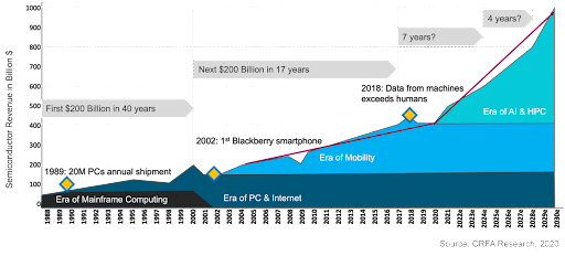
Figure 1. Each successive era of computing is evolving orders of magnitude more quickly than the one before, with HPC and AI driving the semiconductor industry toward the $1T mark by 2030.

Q.What are some of the specific HPC trends, and why are they pushing SoC test forward?

A. The technical trends for HPC illustrate the growing level of complexity in these applications. Key trends include: the rise of chiplets, which we’re seeing everywhere; new Arm server CPUs; larger packages for smaller nodes, which are being ramped by computing rather than mobile devices; 3D package constructs, from micro bumps to hybrid bonding; heightened power and thermal demands created by power supplies; and massive communication challenges created by very large, high-speed data networks.

Data centers, one of the primary applications for HPC chips, are essential for training and operating AI models, which are being employed for everything from autonomous driving to advanced chatbot assistants. In turn, this requires access to the tens of thousands of graphical processing units (GPUs) needed to analyze high volumes of data in real time.

All of these developments together create massive data requirements that result in new test demands to accommodate this 100x rise in complexity, which is pushing the ATE market toward US$10 billion by the end of the decade, as shown in Figure 2.


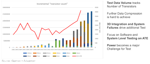
Figure 2. Fast-growing device complexity is driving the market size for ATE. These indicators point to the total available market reaching US$10 billion by 2030.

Q. HPC processors have a longer product development cycle than those for, say, smartphones. At what point in this process does test become critical?

A. During the early phases of product development, semiconductor manufacturers are focused on improving productivity while optimizing techniques essential to functionality. The need for test is particularly high during these early stages. HPC devices are no different in this respect. There are many test needs associated with ramping new nodes, and next-generation devices are always in development. While test is most critical during early development to achieve desired functionality and eliminate bugs, test needs will be consistently distributed across the lifetime of new and emerging devices.

Q. How has the V93000 contributed to Advantest securing its strong market position in SoC?

A. We’re addressing these complex demands with the latest offshoot of our flagship V93000 platform, the V93000 EXA Scale. Establishing V93000 as a scalable platform has allowed us to continually expand its range and functionality to accommodate testing devices for a wide range of applications. This flexibility is a core element of the V93000’s long-term success. We were also the first ATE company to establish long-term compatibility with a single test platform – this is crucial for customers migrating to the next generation of test capabilities. In addition, through our market leadership and customer relationships, we understand what lies ahead for the industry so that our R&D efforts continue to stay on top of HPC requirements.

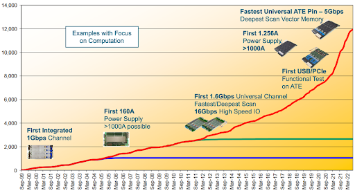
Figure 3. Advantest has continually developed industry-first HPC-level capabilities for the V93000 SoC test platform.

Figure 3 illustrates the evolution of our leadership in HPC innovations, highlighting some of our computationally focused developments. One of the more recent of these developments is the XPS256 device power supply (DPS), which scales from milliamps to more than 1000 amps, covering all power requirements in a single DPS card. We are seeing a number of existing V93000 customers make the transition to EXA Scale for the system’s inherent capabilities as well as options such as the XPS256 and the Pin Scale 5000. When configured with these cards, the EXA Scale system is well equipped to meet exascale computing requirements for mobile, AI, HPC and other advanced devices.

Q. What else should readers know about HPC test requirements and how Advantest is addressing them?

A. Efforts to continue extending Moore’s Law rest on 3D integration – chiplets, stacked packages, FinFETs, etc. This technology is vital to the future of the industry, and it also generates new and different failure types that we have not seen before, necessitating new test approaches and faster testers. EXA Scale is the only tester that can reach 5Gbps on every pin and also has the deepest ATE memories, allowing it to deal with this advanced complexity. In addition, the XPS256 is fully integrated with the EXA Scale system and digitally controlled, so different channels can all be connected by a digital bus, so they can all be kept synchronized and completely controlled by the computational paths inside the system, with no analog factors. This has never been done before, and it allows us to be faster and much more precise in terms of controlling the voltage as well as protecting the device or the probe card. If something goes wrong, we can switch off immediately.

In addition, customers can execute software and interact with their systems via our Link Scale family of digital channel cards for the V93000 platform, which enables software-based functional testing and USB/PCI Express (PCIe) scan testing of advanced semiconductors. The card essentially behaves like your computer, communicating with the device under test through a standard high-speed serial interface to enable very fast transfer of functional and scan test content. Because the device can be interacted with on the wafer the way they’ll be used later on when they’re singulated and packaged, the user can increase test coverage and throughput simultaneously as well as realize faster time to market. 

As new HPC computing developments arise, Advantest is well-positioned to address concurrent test needs through our V93000 platform and continually expanding portfolio of best-in-class cards and peripherals.

Read More

Posted in Top Stories

Deploying Cutting-Edge Adaptive Test Analytics Apps: Innovation Based on a Closed-Loop Real-Time Edge Analytics and Control Process Flow into the Test Cell

By Ken Butler, Senior Director of Business Development, Advantest, & Guy Cortez, Senior Staff Product Manager, Synopsys

Semiconductor test challenges abound in this era of AI. As such, semiconductor test engineering is increasingly moving towards fully adaptive test where each device receives the “right” test content to assess its correctness. Advantest and Synopsys have partnered to provide new cutting-edge real-time adaptive test applications at the test cell based on complete closed-loop analytics and control process flow. Our solution leverages a high-performance, highly secure real-time data infrastructure combined with advanced analytics derived from a comprehensive silicon lifecycle management (SLM) platform. For example, when test measurement data is combined with on-die sensor readings using a very fast and secure computing platform, the solution provides an in-situ adaptive test with milliseconds latencies.

Figure 1. Semiconductor test challenges for the AI era

First, let’s review the Advantest ACS portion of the solution. The Advantest ACS Real-Time Data Infrastructure (RTDI) is a platform that provides low latency and highly secure data access and system control for test operations (Figure 2). It consists of the following components:

  • ACS Container Hub™, a web registry for the management and distribution of open container initiative-compliant AI/ML and statistical workloads.
  • ACS Unified Server™, a multi-purpose, reliable and scalable platform that serves as a gateway and local mirror for containerized applications.
  • ACS Edge™, a high-performance and highly secure computing solution for the execution of complex analytical workloads for real-time applications in production test.
  • ACS Nexus™, the communications backbone for ACS RTDI which allows for streaming access to test and test cell data as well as real-time control of tester operations.


Figure 2. ACS Real-Time Data Infrastructure

Two example use cases to which adaptive test flow can be applied are:

  1. Reduce test time – Save cost and improve throughput by eliminating some tests that appear useless (no parts failing).
  2. Reduce DPPM – Improve quality control by adding additional tests for some “risky” parts.

Our first use case focuses on this second method of improving quality. Figure 3 below is an image of a stacked wafer map that highlights specific zonal regions on the wafer that have an excessive number of failures, shown in purple. A typical stacked wafer map consists of 25 wafers or one lot’s worth. The remaining good die in this region are suspect due to the amount of failures on this part of the wafer. The larger and darker the purple identifier per x, y coordinate is, the more prominent failures there happen to be at that x, y coordinate across all wafers analyzed.

An application is available to identify which packaged die from select x, y coordinates are considered risky based on a specific failure threshold set by the product engineer. Additional test(s) will later be applied to those parts labeled as risky during final test (a form of ZPAT at final test), thereby improving the overall quality of the chip but with minimal impact on total test time.

Figure 3. Wafer stack map

A second application is adaptive limit setting, i.e., the adjustment of test limits during test program execution. The method shown here utilizing sensor data provides higher accuracy in limit management compared to existing methods such as dynamic part average testing (DPAT), because sensors embedded in the chip provide additional key information that enables the monitoring of the chip’s operational metrics such as power and performance. This example highlights the use of sensor data that characterizes the process and environment information to enable more accurate limits on speed/power consumption during testing, thus resulting in lower DPPM and higher quality.

Figure 4 below shows a comparison of the two adaptive test limit approaches. First, the DPAT method shown is a standard univariate approach based on the die population results for a given test. Next, the sensor-aware method incorporates a bivariate correlation between the data measured from sensors and the results of a specific VDD consumption test. The second method can identify at-risk die that would be missed by conventional DPAT analysis.

Figure 4. Traditional univariate DPAT vs. sensor aware bivariate method

Conclusion: In this article, we describe a real-time, highly secure data infrastructure plus a pair of complex, high-value analytical applications that consume both test response and on-die sensor data to produce inferences for true adaptive test decision-making with low milliseconds latencies. The analytics and associated applications are available as part of an open solutions ecosystem, which allows users to either develop their own solutions or procure and deploy them from Synopsys or other providers. The result is the democratization of machine learning driven applications, making them available to everyone in the semiconductor test community.

Related Links:

The Advantest ACS Solution Store

Advantest ACS

Advantest Talks Semi Podcast

Read More

Posted in Top Stories

Scalable Platform Meets the Test Challenges of Ultra-Wideband Chipsets

This article is adapted from a paper and presentation at SEMICON China, March 2023.

By Kevin Yan and Daniel Sun, Advantest (China) Co., Ltd.

Ultra-wideband (UWB) technology, as defined by IEEE 802.15.4 and 802.15.4z standards, enables short-range, low-power RF location-based services and wireless communication. A variety of devices have reached the market to help implement UWB capability, but these devices present significant test challenges related to the high RF frequencies at which UWB operates, the ultrawide bandwidths of UWB’s multiple channels, and the technology’s complex modulation schemes. An effective test platform requires flexibility and scalability to handle the frequencies and bandwidths involved, as well as the compute power to effectively analyze the test results.

UWB markets and capabilities

The UWB market is expanding at a rapid pace. One forecast estimates that UWB unit shipments are growing at a 40% CAGR with the market for UWB chips expected to reach $1.259 billion by 2025.1 UWB serves both business and consumer end markets, with the consumer segment now representing the majority. UWB is hitting the mainstream in the mobile smartphone market, with the automotive and wearables/tags segments also seeing UWB adoption.

Some specific applications that UWB can serve include indoor navigation, item tracking, secure hands-free access, credential sharing, and hands-free payments. In addition, automotive applications are likely to expand, with the Car Connectivity Consortium incorporating UWB into the Digital Key Release 3.0 specification currently under development. 

Compared with other technologies, UWB provides superior positional accuracy. Table 1 compares UWB with RFID, Wi-Fi, and Bluetooth. UWB, which employs time of flight (ToF) and angle of arrival (AoA) technology, achieves a positional accuracy of better than 30 cm, outperforming the others. Bluetooth incorporates AoA and angle of departure (AoD) to provide < 1 m of accuracy (version 5.1). Wi-Fi, which relies only on its Received Signal Strength Indicator (RSSI) functionality for distance estimates, has a limited accuracy of 15 m. RFID can only detect presence, not distance.

Table 1. Positional accuracy comparison of four wireless technologies

UWB basics

The United States Federal Communications Commission (FCC) and the International Telecommunication Union Radiocommunication Sector (ITU-R) define UWB as a communications technology that transmits and receives a signal whose bandwidth exceeds the lesser of 500 MHz or 20% of the arithmetic center frequency fc. The UWB physical (PHY) layer includes 16 channels in three groupings, as shown in Table 2. The sub-gigahertz band (group 0, shaded yellow) includes one channel at an fc of 499.2 MHz, the gigahertz low band (group 1, shaded blue) includes four channels with fc ranging from approximately 3.5 GHz to 4.5 GHz, and the gigahertz high band (group 2, shaded red) includes 11 channels with fc extending from approximately 6.5 GHz to 10 GHz.

Table 2. UWB PHY group and channel allocation                

Most UWB products currently on the market focus on the high band, particularly channels 5 and 9. The UWB PHY layer also comes in low-rate-pulse (LRP) and high-rate-pulse (HRP) repetition-frequency configurations. HRP high-band configurations are becoming the preferred configurations, finding success in industrial applications for location and ranging and for device-to-device communications. Table 3 outlines the IEEE 802.15.4z HRP UWB high-band specifications, including a range up to approximately 100 m and data rates from 110 kbps to 27.4 Mbps. In addition, HRP UWB uses two types of modulation: burst position modulation (BPM) and binary phase-shift keying (BPSK).

Table 3. IEEE 802.15.4z HRP UWB high-band specifications

Figure 1 compares the UWB and Bluetooth spectrums. The narrow-band Bluetooth (left) has a 1 MHz bandwidth at 2.4 GHz. In contrast, UWB (right) has a 500 MHz or greater bandwidth at center frequencies (fc) extending up to approximately 10 GHz, as shown in Table 1. Each band’s upper and lower bounds (fH and fL, respectively) exhibit power levels 10 dB less than the maximum power level at fc.


Figure 1. Bluetooth has a 1-MHz bandwidth at 2.4 GHz, while high-band HRP UWB has a > 500-MHz bandwidth at center frequencies fc from approximately 6.5 GHz to 9.5 GHz.

Test requirements

A typical UWB transceiver chipset includes an analog front end containing a receiver (Rx), a transmitter (Tx), and a digital backend that interfaces to an off-chip host processor. It also includes a Tx/Rx switch that connects either the receiver or transmitter to an antenna port. Some versions come with two RF antenna ports to serve phase-difference AoA applications, and some will add even more ports to improve positional accuracy. AoA capability can help pinpoint the specific location of an object as well as its distance, as shown in Figure 2.


Figure 2. AoA capability can help pinpoint a tag’s angular location as well as distance.

The receiver includes an RF front end that employs a low-noise amplifier that amplifies the received signal before down-converting it to the baseband. The chipset’s transmitter applies digitally encoded transmit data to an analog pulse generator. The chipset also includes a phase-locked loop (PLL) that provides local oscillator signals for receive and transmit mixers.

Typical UWB production tests involve transmit measurements and pulse-related measurements as specified in the 802.15.4z standard as well as direct receiver measurements, ToF measurements, and AoA measurements. 

Transmit measurements ensure the devices meet all emissions rules established by the FCC or other relevant governmental authorities. The tests involve power spectral density (PSD) measurements in accordance with a transmit-spectrum mask (Figure 3) as well as center-frequency tolerance measurements.


Figure 3. A power spectrum mask defines limits for PSD measurements.

Pulse-related measurements ensure the interoperability of UWB devices and are performed using time-domain analysis (Figure 4). Specific tests include baseband impulse response, including measurement of pulse main-lobe width, pulse side-lobe power, and normalized mean square error (NMSE). Additional tests look for chip clock error and chip frequency offset. 


Figure 4. This compliant pulse example uses time-domain analysis.

Although not specified in the 802.15.4z standard, direct receiver measurements must be performed to ensure quality parts. A typical receiver test measures the minimum power level at which the device can operate with minimum error. A typical way to perform this test is to send a minimum power stimulus to the device under test and measure the device’s packet error rate (PER).

Finally, ToF and AoA measurements characterize the positioning performance. In high-volume production test, such measurements are often performed using phase shifts between two Rx antenna inputs.

UWB devices present three specific test challenges that traditional ATE systems cannot address. The first relates to the high RF frequencies involved, ranging up to more than 10 GHz—exceeding the typical less-than 6 GHz capability of many traditional ATE RF instruments. Second, UWB devices require wideband measurements extending to 1.35 GHz—well beyond the 200 MHz limits of traditional instruments. Third, UWB devices must be tested using frequency-domain PSD measurements and time-domain impulse-response measurements, a combination that requires test software with complex algorithms and an efficient architecture to handle the huge amounts of data processing required.

UWB test platform

The flexible Advantest V93000 platform can be configured with appropriate hardware and software to support the thorough test of UWB devices. The platform’s Wave Scale RF instruments cover the frequency range from 10 MHz to 70 GHz. The V93000 platform can also support the necessary wide bandwidths. For example, the Wave Scale RF18 card supports 5.85 GHz to 18 GHz frequency stimulus and measurements with a 200 MHz bandwidth. Adding the optional Wave Scale Wideband card to the Wave Scale RF18 extends the bandwidth up to 2 GHz. The combination also has built-in event triggering—useful for testing asynchronous UWB chips’ Tx packets. The platform can accommodate 128 RF ports to enable efficient multisite parallel testing.

V93000 SmarTest 8 software contains a UWB demodulation library and can analyze a UWB signal in the time and frequency domains and measure such items as the transmit PSD mask, transmit center-frequency tolerance, baseband impulse response, chip clock rate, and chip carrier alignment. To enable rapid test-data analysis, SmarTest 8 supports hidden uploads of captured waveforms and multi-threaded background processing of previously captured data while simultaneously capturing the next measurement. In addition, standard existing SmarTest 8 features can make receiver and ToF-related measurements. Finally, AoA tests can be performed by signals of different phase to different receiver ports, as shown in Figure 5.


Figure 5. AoA tests require relative phase measurements between antenna receiver ports in response to applied stimulus from V93000 instruments.

Conclusion

As the UWB market rapidly expands, test platforms are adapting to accommodate the high RF frequencies, wide bandwidths, and complex modulation schemes involved. The Advantest V93000 platform’s hardware and software include the standard and UWB-specific features necessary to test UWB devices.

Acknowledgments

We would like to acknowledge and give our warmest thanks to Frank Goh, who supports the UWB V93000 Solution and provided professional guidance to this paper. Frank Goh is a principal consultant at the Center of Expertise Asia from Advantest Singapore.  

Reference


  1. AMENDED Comments of The Ultra Wide Band (UWB) Alliance Before The Federal Communications Commission, July 14, 2020.
Read More

Posted in Top Stories

True Zero Trust Combats IC Manufacturing Security Challenges

By Michael Chang, ACS VP and General Manager

The semiconductor manufacturing industry is facing a host of unprecedented technology and security challenges. A common catchphrase these days is that “data is the new oil.” Data is everywhere, in everything we do, and there is both good and bad associated with this trend. Data everywhere creates new security issues that need to be addressed to protect the integrity of your information and your devices. Advantest has done this through a new infrastructure setup that enables a True Zero Trust environment on the fab test floor – in turn, allowing us to truly embrace AI without having to fear security repercussions.

Addressing core challenges

Some of the key technology challenges for chipmakers include chip-level scale integration, which requires new types of setup tools and data to be integrated for making measurements; system quality challenges; and achieving chip-scale sensors. Another area of focus is manufacturing 2.5D and 3D chiplets.

A paper published in 2021 by three Google engineers identified an issue with cores failing early due to fleeting computational errors not detected during manufacturing test, which they call “silent” corrupt execution errors. The paper goes on to propose that researchers and hardware designers and vendors collaborate to develop new measurements and procedures to avoid this problem. The interim solution is to isolate and turn off cores that are failing, but they hint that because of chip-level integration and 2.5D/3D, new approaches are needed to measure and screen out these failing cores automatically.

The other side of this coin is security concerns. Access to systems is limited, and different software cannot be installed on machines. We use firewalls, anti-virus spyware, encryption, password management and other technologies to protect our computers, but they’re not infallible. Experts agree that cyberattacks are inevitable, so there needs to be a means of using data to protect all the data on our systems. Advantest is doing this through our ACS offerings, which enable real-time data security, as shown in Figure 1: ACS Nexus™ for data access, ACS Edge™ for edge computing, and the ACS Unified Server for True Zero Trust™ Security.

Figure 1. Advantest’s open solution ecosystem. Data is needed from all sources to mitigate new challenges.

As Figure 1 illustrates, through our Real-Time Data Infrastructure, we can integrate data sources from across the chip manufacturing supply chain, leveraging that data to continually improve our insights and solutions. We can implement test throughout the product lifecycle, taking real-time action during production. Nothing has to be done away from the test floor; all analyses and actions occur during actual test, maintaining fully secure zero trust protection of the data.

Security is more than protection

One way to illustrate the approach that we take to security in semiconductor manufacturing is to look at a seemingly unrelated example: the International Space Station (ISS). Designed to protect against damage from space debris, the outer hull of the ISS is outfitted with Whipple bumpers. These multi-layered shields are placed on the hull with spaces between the layers. The intent is that impact with a layer will slow and, ideally, break apart the projectile, so that by the time it reaches the bottom layer, any potential harm has been prevented. While the bumpers slow the kinetic energy of the debris, something will eventually get through. The second line of defense is the ISS’s containment doors, which ensure any areas where air leaks have been detected can be isolated so that the astronauts are protected. Clearly, this is mission-critical.

The key word: “containment.” It’s not enough to protect – no system is infallible. You also have to contain it so that potential security issues don’t become pervasive and cause a major breach. The challenge when looking at this from the test cell perspective is the test cell is located on the test floor, which is surrounded by all kinds of other equipment that you have no control over. And not just other manufacturing tools. Everyday office products can be vulnerable to hacking – computers, software, printers, routers… even smart appliances in the break room such as IoT-enabled coffee pots. Hackers are increasingly finding ways to get to us through software update servers, routers, printers, and even bypassing firewalls.

Figure 2. The ACS-enabled True Zero Trust environment for the test floor is a must to ensure containment.

The bottom line is that your infrastructure is going to be vulnerable, so you must add a reliable containment structure such that, when there is an attack, you can shut down. This is what our True Zero Trust™ environment is designed to enable. The “zero trust” concept is just what it sounds like – the complete elimination of the assumption of trust from within networks and systems. This means that no default trust is granted to any user or device, either inside or outside an organization’s network. This model grants resource access on a need-to-know basis only, requiring stringent identity verification and contextual information that cannot be known or provided by another source. By preventing unauthorized access to sensitive data, companies mitigate the risks of data breaches and attacks, whether external or internal.

What does this mean for AI/machine learning?
New chip technologies require new measurements, relying on multi-dimensional data. Large language models (LLMs) are creating vast new opportunities in all domains. LLMs are machine learning models that can perform natural-language processing tasks such as generating and classifying text, answering questions, and translating text. LLMs are trained on massive amounts of text data and use deep learning models to process and analyze complex data. This can take several months and result in a pretty hefty power bill.

However, during training, LLMs learn patterns and relationships within a language while aiming to predict the likelihood of the next word based on the words that came before it. We’re talking about a very large number of parameters and petabytes of data. LLMs are used in a variety of fields, including natural language processing, healthcare, and software development.

Currently, LLMs can comprehend and link topics, and they have some understanding of math. But an app like ChatGPT – the most popular and widely used LLM – does not understand new developments as it is not connected to the Internet. LLMs can recognize, summarize, translate, predict, and generate human-like texts and other content based on knowledge from large datasets, and they can perform such natural-language processing tasks as:

  • Sentiment analysis
  • Text categorization
  • Text editing
  • Language translation
  • Information extraction
  • Summarization

Using LLMs to summarize knowledge and feed it into the test cell or test floor can be done in a True Zero Trust environment because there is no danger of the data being manipulated in undesirable ways. With that said, LLMs aren’t self-aware – they don’t know when they make mistakes, so an LLM should be considered a data exoskeleton.

Conclusion 

Over the next few years, we can anticipate a significant shift in the types of applications being developed, moving away from traditional statistical machine learning and towards more sophisticated autonomous or semi-autonomous agents that can automate testing. In order to effectively safeguard the valuable assets and intellectual property of OSAT and fabless organizations, containment is necessary. The ACS Real-time Data Infrastructure offers a highly secure containment system called True Zero Trust. Through its innovative design, this infrastructure establishes a cutting-edge paradigm that allows for the creation of secure data highways and paves the way for building novel applications with enhanced security.


Read More

Posted in Featured

Advantest Talks Semi: Harness AI power for yield, quality and reliability

Today’s semiconductor manufacturing landscape is riddled with escalating complexity, contracting process nodes, and amplified demands for rigorous quality control. These challenges have a profound impact on cost and time-to-market.  

 To confront these issues head-on, Advantest, proteanTecs, and PDF Solutions have formed a strategic alliance. Not only is this collaboration geared towards mitigating current challenges, but it is also strategically positioned to future-proof the semiconductor manufacturing process.   

 In this installment of the “Advantest Talks Semi” podcast, we discuss how this alliance enhances manufacturing processes, ensuring superior quality, increased reliability, and better yields. All of these efforts are directed towards achieving reduced costs and expedited time-to-market.  

https://www.buzzsprout.com/1607350/12911337

Read More