Pages Menu
TwitterRSSFacebook
Categories Menu

Posted in Featured Products

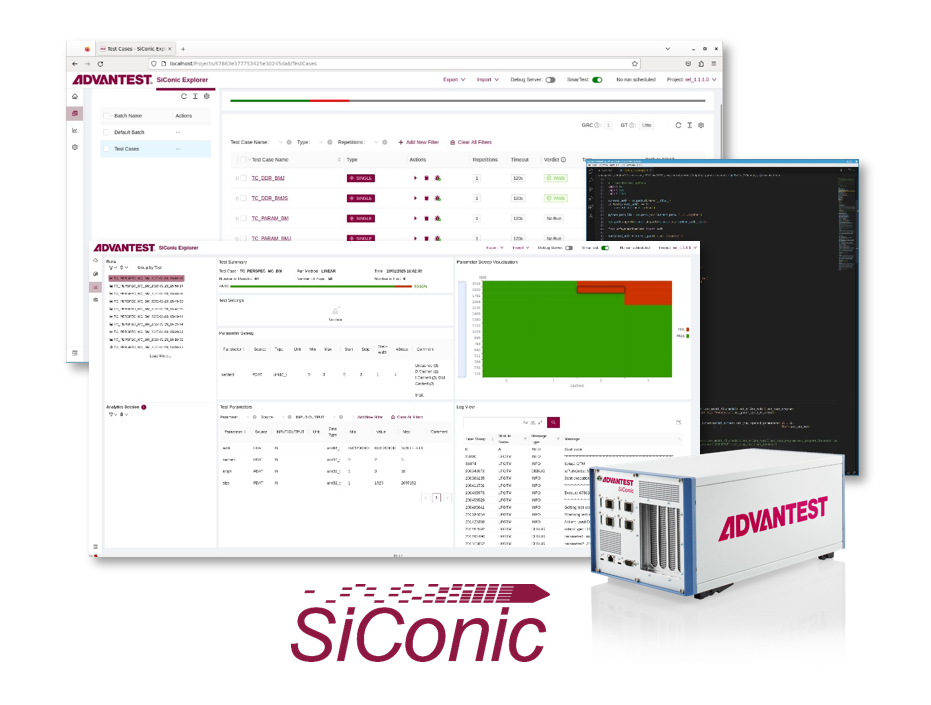
Advantest Unveils SiConic™ Test Engineering: Unified, Scalable Bench Environment for Debug and Validation

In May, Advantest unveiled SiConic™ Test Engineering (TE), the newest addition to the SiConic™ family introduced in February 2025. SiConic TE offers test engineers the ability to bring up and validate structural and functional tests over high-speed I/O (HSIO) interfaces in a scalable bench environment, enabling earlier validation and debug without occupying valuable ATE systems.

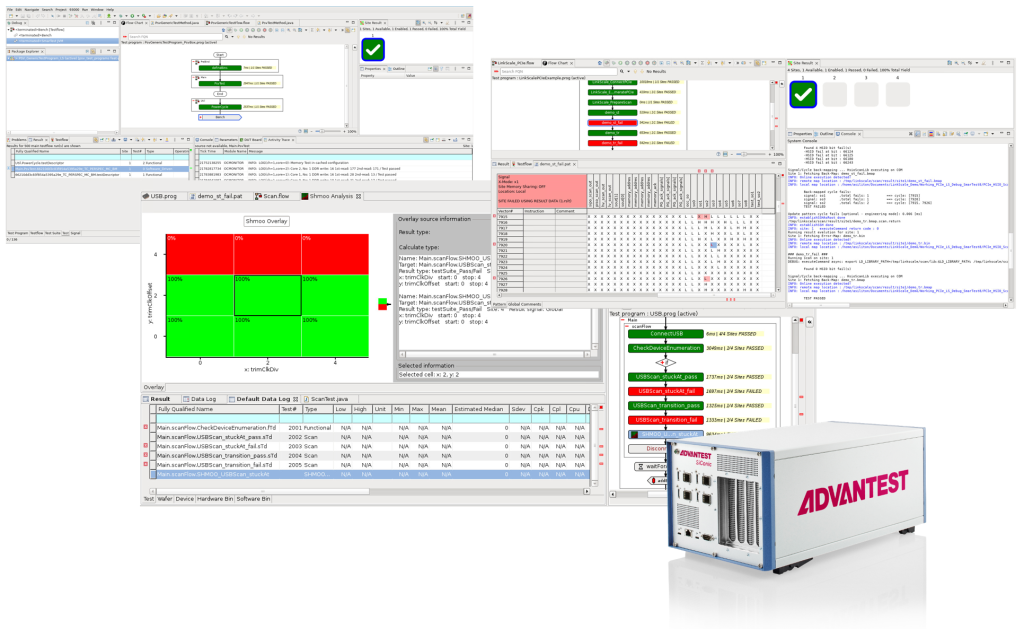
SiConic Link flexibly connects to standard evaluation boards through functional interfaces like USB, PCIe, control interfaces, and GPIOs. This is the foundation for SiConic TE to enable test engineers to rapidly validate and debug design verification (DV) and design for test (DFT) content in SiConic’s unified environment on the bench.

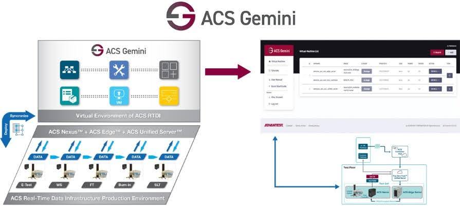
Building on V93000 leadership in scan over USB or PCIe, SiConic’s unified environment brings native DV test content to test engineering without the error-prone and lengthy conversion and debug cycles typical for bring-up of advanced functional tests on ATE. These tests are required for high-quality test coverage in verification and test, enabling a productivity boost for the bench collaboration of DV, DFT and test engineering. SiConic TE accelerates time-to-quality for both V93000 as well as Advantest’s SLT and burn-in platforms with the ActivATE360™ suite of software tools.

Integrating seamlessly with SiConic Link hardware and the SmarTest 8 software platform, SiConic TE provides users with comprehensive access to functional HSIO links for enhanced throughput and rich trace capabilities during test execution. By enabling smoother handoffs between silicon validation (SV), DV and TE teams, SiConic TE fosters tighter cross-domain collaboration.

Through its unified test environment and shared ecosystem, SiConic TE improves the correlation between bench, ATE and SLT systems. The tool’s optimized engineering resources allow bring-up and debug to be offloaded from ATE to the bench, freeing up valuable tester capacity and enabling more effective scaling. In addition, tight integration with leading EDA partners enables cross-functional collaboration with DV and DFT teams, improving test content development and speeding first-silicon success.

According to G. Dan Hutcheson, vice chair, TechInsights, “Improving productivity at the R&D level is vital for design engineers. Advantest’s automated silicon validation approach would allow sign-off and test engineering to proceed concurrently using shared test data, helping ramp SoC designs more quickly, and shortening time-to-money, while ensuring design-to-system quality.”

Industry Support

Advantest developed SiConic TE in close collaboration with leading customers and EDA partners to ensure seamless integration into existing design and validation flows.

“Siemens EDA and Advantest have a long history of joint development on many DFT technologies, including Tessent Streaming Scan Network (SSN) and IJTAG,” added Ankur Gupta, senior vice president and general manager, Digital Design Creation Platform, Siemens EDA, Siemens Digital Industries Software. “Collaborating on Advantest SiConic and Tessent In-System Test strengthens this long-running collaboration and helps to provide our users with time-to-market improvements and higher productivity.” 

“As the scale and complexity of chips continues to increase, new verification approaches are needed to shift verification cycles earlier and deliver silicon with higher quality,” said Tom De Schutter, senior vice president of product management at Synopsys. “Our collaboration with Advantest enables users to develop drivers for high-speed interfaces, validate SERDES and perform functional testing and structural testing through the combination of Advantest’s SiConic platform and Synopsys’ HAPS-100 platform, VC Portable Stimulus, TestMAX SF/SEQ and SLM HSAT IP solutions.”

More information:https://www.advantest.com/en/news/2025/20250508.html

Read More

Posted in Featured Products

Advantest Introduces SiConic: Groundbreaking Solution for Automated Silicon Validation

This past February, Advantest unveiled SiConic: a scalable solution for automated silicon validation. Designed to address the increasing complexity of advanced systems-on-chip (SoCs), SiConic enables design verification (DV) and silicon validation (SV) engineers to achieve faster sign-off with unparalleled reliability, efficiency and collaboration. SiConic signals Advantest’s commitment to transforming the R&D process for its customers.

The semiconductor industry is facing unprecedented challenges. Growing SoC design complexity, together with the adoption of 3D packaging and heterogeneous integration, is straining traditional validation workflows. DV and SV teams are under pressure to reduce time-to-market and time-to-quality – even as more devices with more intricate features are being developed within constrictive timelines. Reusing the wealth of verification content developed in pre-silicon would provide an efficiency and quality breakthrough. However, the industry lacks the automated flow and tools to reliably re-use and extend verification tests for silicon validation. SiConic’s ecosystem – including EDA partners such as Cadence, Siemens and Synopsys – overcomes this barrier to reuse, enabling engineering efficiency and accelerated test execution on real silicon.

SiConic Explorer, the platform’s software backbone, offers an automated flow by integrating seamlessly with EDA verification tools based on the Accellera Portable Test and Stimulus Standard (PSS), e.g., the Cadence Perspec System Verifier. In addition, integration with debuggers, such as Lauterbach’s TRACE32 debugging tool, accelerates the bring-up of complex multi-IP test cases.

SiConic Link is the hardware foundation of the SiConic solution on a bench. With its high-speed I/O (HSIO) capability, SiConic Link supports protocols such as PCIe and USB to enable functional validation with high throughput and rich tracing capabilities during test execution. The test instrument provides control interfaces (e.g., JTAG, SPI) and general-purpose I/Os, improves the debugging workflow and provides extensive control and observability of the device in its target board environment.

With SiConic, DV engineers can now leverage familiar pre-silicon techniques, expanding their functional coverage in post-silicon. Similarly, SV engineers benefit from seamless load, set parameters and debug of PSS-based or manually directed content on silicon, thereby enabling rapid and reliable device bring-up and functional characterization. The highly portable solution can be easily scaled for use by distributed global R&D teams collaborating on a complex SoC with diverse IP blocks. SiConic enables confident sign-off decisions through team collaboration and data-driven insights – building trust with customers receiving early samples and expecting reliable ramp and operation during the lifetime of their systems.

Read More

Posted in Featured Products

Advantest Unveils T5801 Ultra-High-Speed Memory Test System to Power Next-Generation DRAM Devices

Early this year, Advantest announced the T5801 Ultra-High-Speed DRAM Test System. The cutting-edge platform is engineered to support the latest advancements in high-speed memory technologies —including GDDR7, LPDDR6, and DDR6 — critical to meeting the growing demands of artificial intelligence (AI), high-performance computing (HPC), and edge applications. 

Increasingly complex, high-speed memory technologies are pushing the boundaries of data center and AI performance. The T5801 is tailored to address this challenge by enabling accurate and efficient mass production testing for the highest-speed memory devices. Featuring an innovative Front-End Unit (FEU) architecture, the system is uniquely equipped to handle the rigorous requirements of next-generation DRAM modules, delivering industry-leading performance of up to 36Gbps PAM3 and 18Gbps NRZ. 

The T5801 builds on Advantest’s market leadership in DRAM test solutions, including the proven T5503 series and V93000HSM systems. Its support for PAM3, a first in JEDEC-standard DRAMs, highlights the system’s capacity to handle memory innovations such as GDDR7, which is central to achieving ultra-low latency in all AI environments. Its scalable testing infrastructure enables a seamless transition from engineering R&D to production, offering flexible configurations and full compatibility with existing handlers and interfaces

Read More

Posted in Featured Products

Advantest Launches KGD Test Cell for Power Semiconductors

Late last year, Advantest announced an integrated test cell designed to maximize die-level test yields for wide-bandgap (WBG) devices essential to power semiconductors. The Advantest Known Good Die (KGD) Test Cell combines the company’s CREA MT Series power device testers with the new HA1100 die prober. 

Demand for power semiconductors continues to grow with the rapid escalation of electric vehicles (EV) and power infrastructure. WBG devices, particularly silicon carbide (SiC) and gallium nitride (GaN), are essential for the design and manufacture of power semiconductors, enabling them to be smaller, faster, and more efficient than silicon-based devices. However, failure screening of WBG devices is challenging, as the probe card, the chuck, and the devices can be damaged due to the devices operating at very high voltage and current. 

Essentially serving as a one-stop shop for efficient equipment management, the Advantest KGD test cell solution helps reduce customers’ manufacturing costs. CREA’s proprietary probe card interface (PCI) technology can eliminate damage risk. Even if damage issues occur, Advantest will investigate it with the test cell. Customers can minimize the downtime of the test cell. The HA1100 die prober for the CREA MT Series test systems enables assembly of dies in power modules using only passed (KGD) die, ensuring no failed die find their way into the module. This prevents yield loss at module test, thus reducing the loss of final multi-die assembled power modules.


Read More

Posted in Featured Products

Advantest Launches ACS Gemini™ – New Developer Platform for Accelerating ACS RTDI™ Application Development

Last December, Advantest announced the launch of its new software development platform ACS Gemini™, which allows customers to develop, simulate and debug machine learning applications in a virtual environment. The digital twin of ACS RTDI™, ACS Gemini is part of Advantest’s mission to enable customers and partners to utilize data analytics in developing artificial intelligence (AI) and machine learning (ML) solutions for semiconductor testing. 

In recent years, manufacturing costs for semiconductors have increased significantly due to their growing complexity. Analysts at McKinsey & Company predict that implementing AI and ML could lower manufacturing costs by 40%, as many engineers use these technologies to optimize efficiency in manufacturing. 

ACS Gemini improves efficiency by providing customers with a seamlessly integrated experience that optimizes design-to-production proficiency in the virtual ACS RTDI environment. The digital twin software solution is composed of the ACS Software Development Kit, Reference Application Development Model, and Containerized applications publishable to the ACS Container Hub™. These elements enable customers to simulate valuable test results in a virtual production setting. 

ACS Gemini saves customers time and cost in engineering debugging, design vs. production correlation, and cloud deployment of apps—ultimately saving valuable tester time. Overall, the solution accelerates ML application development, simulates testing results, and shortens time-to-deployment of ML applications on the production test floor. 

Advantest’s ACS RTDI is a real-time data infrastructure platform-as-a-service that securely collects, analyzes, stores and monitors semiconductor test data to empower customers to automate the process of converting insights into actionable test decisions within milliseconds. This helps customers and partners reduce test time, optimize quality and reliability and enhance smart packaging.

Read More

Posted in Featured Products

Advantest Rolls Out Wave Scale RF20ex: High-Frequency, High-Bandwidth RF IC Test Card for the V93000 EXA Scale Platform


Earlier this month, Advantest unveiled the Wave Scale RF20ex instrument for the V93000 EXA Scale platform. It enables customers to test virtually any type of radio frequency (RF) device using a single instrument. Wave Scale RF20ex takes the innovations of the V93000 Wave Scale RF solution to a new level, providing double the number of RF ports per instrument and offering future-proof frequency and bandwidth coverage with a frequency range of 100MHz to 20GHz and an industry-leading 2GHz bandwidth capability. It is well equipped to address 5G, WiFi-7, ultra-wideband (UWB) and any other current or future standards in RF.

As semiconductors continue to evolve toward higher performance, technology convergence and complexity, a broader and more integrated test solution is needed. The new Wave Scale RF20ex provides a unified, single-card solution for all standard RF applications. For UWB applications, Wave Scale RF20ex on the V93000 platform enables ATE for a new class of devices that are more demanding in their testing requirements in terms of modulation bandwidth and frequency coverage while driving higher levels of multi-site test and lower cost-of-test (CoT). 

“Our intent in developing Wave Scale RF20ex is to offer the best-in-class instrument for RF ATE with the best available operational efficiency,” said Ralf Stoffels, executive officer and division manager of Advantest’s V93000 product unit. “This single card improves performance for many applications while simplifying configurations that can cover the entire RF market—with built-in capability to also handle the forthcoming WiFi-8 and 6G device generations.”

Wave Scale RF20ex Key Features

The Wave Scale RF20ex card offers a wealth of features and benefits engineered by Advantest RF test experts, including:

  • 64 bi-directional ports per card
  • 100MHz – 20GHz coverage on all ports
  • 2GHz of instantaneous bandwidth for stimulus and measurement

Read More