Pages Menu
TwitterRSSFacebook
Categories Menu

Posted in Top Stories

System-Level Test Essential for Fast-Growing Embedded NAND Market

By Ken Hanh Duc Lai, Marketing Director, Advantest America

The market for NAND flash memories is growing at a rapid pace, driven in large part by the massive demand for solid state drives (SSDs), which have replaced hard disk drives for many applications. According to Gartner, the SSD market will reach above 370 million units in 2020, and IC Insights forecasts that memory IC products will show the strongest growth rate through 2021 of the four major IC product categories (the others being logic, analog and microcomponents).

A significant portion of the SSD market is commanded by PC servers and clients used for big data storage applications. However, the mobile market comprising portable wireless devices like smartphones and tablet PCs is growing as well, with variations in form factor increasing to meet new market demands. Driven by these applications, mobile memory unit shipments are forecast to exceed 2 billion units by 2020. These include embedded multimedia cards (eMMC), embedded multi-chip packages (eMCP), MCP and raw NAND. In concert with this growth, the embedded NAND market is undergoing a shift in protocol usage. Embedded NAND is in 80 percent of the smartphones currently on the market, and while smartphones and tablets have typically used eMMCs to store information, a transition is under way from eMMC to Universal Flash Storage (UFS) as the future of flash memory (see Figure 1).


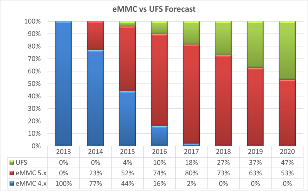
Figure 1. UFS has taken hold, and is expected to represent half the market for NAND flash SSDs by 2020. (Source: IHS Mobile and Embedded Memory Market Tracker Q4 2016)

The JEDEC-defined UFS mobile-centric storage standard addresses next-generation mobile performance and scalability, offering fast sequential read/write speeds with high random IOPS1, which are essential for mobile phones. (For SSDs, random IOPS numbers are primarily dependent upon the storage device’s internal controller and memory interface speeds.) One key value of UFS is its ability to leverage the strengths of several existing technologies in one standard: the low power consumption of eMMC; the MIPI interface standard, M-PHY and UniPro, for the interconnect layer; and the SCSI command set as the application protocol.

Devices based on UFS 2.0, the current version of the standard, offer the highest available performance of any SSD interface standard due to its separately dedicated read/write paths, which enable UFS to read and write simultaneously. At up to 1200 Megabytes per second (MB/s), UFS operates at twice the rate of Serial ATA (SATA) 3.0 and three times that of eMMC5.0. UFS also consumes less total power by processing tasks sooner and staying in standby mode longer. Figure 2 summarizes the key benefits of UFS standard.

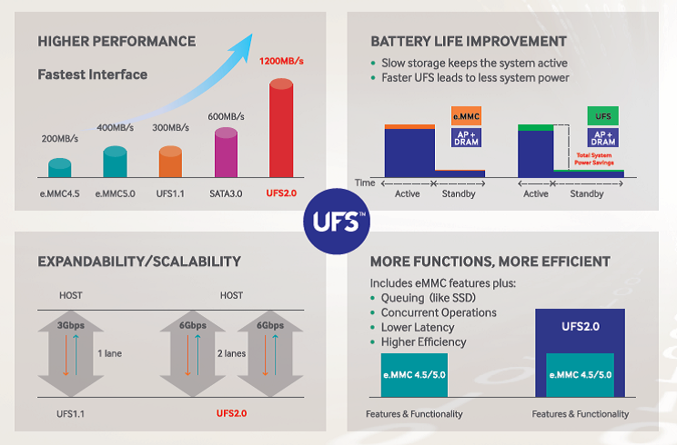
Figure 2. UFS offers a number of benefits that make it a superior option for embedded storage in mobile devices. (Source: Universal Flash Storage Association)

UFS is here

Adoption of UFS in the U.S. has already begun, with most of the top 10 mobile handset OEMs using UFS memory for their flagship models. While this includes primarily high-end handsets at the moment, as the cost to implement UFS continues to decline, more and more mid-tier phones will incorporate UFS-based embedded NAND memory devices. Moreover, the ecosystem for UFS is already in place, with a range of vendors supporting the UFS interface, including makers of NAND flash, systems-on-chip (SoCs), operating systems, measurement tools, and testers optimized for high-volume manufacturing (HVM).

Major NAND makers and manufacturers of UFS and BGA2 SSDs have adopted system-level test (SLT) for production use. More than 50 testers overall have been installed since the second half of 2016 for system-level testing of UFS and BGA SSDs, and this number is expected to triple during 2017.

Flexible tester optimized for embedded NAND

Memory IC makers need a class of tester that specializes in SLT of these devices, while maintaining the reliability, low cost and high volume capabilities required for conventional memory testers. Advantest developed its T5851 system-level test (SLT) solution – part of the T5800 platform series – specifically to meet these needs, delivering cost-effective testing of UFS and BGA SSDs. Built with the same proven test architecture used in Advantest’s MPT3000 family of SSD protocol test solutions, the T5851 allows customers to minimize both their capital investments and deployment risks by using the same platform and FutureSuite™ software as other members of the T5800 product line.

The flexible T5851 tester is available in both production and engineering models, allowing the system to be used for reliability and qualification testing as well as test-program development or, when equipped with an automated component handler such as Advantest’s M6242, high-volume production. As a fully integrated SLT solution, the T5851 provides multi-protocol support in one tool while its tester-per-DUT [device under test] architecture and proprietary hardware accelerator allow it to achieve industry-leading test times.

Currently, Advantest has many T5851 systems installed at IDM3 and OSAT4 customer sites worldwide for HVM production, qualification and engineering. This number is expected to increase as adoption of UFS becomes more widespread. This will be spurred by the release of UFS 3.0, as well as expansion of the standard into other applications, such as memory cards, PC clients, smart TVs, and automotive devices, which are anticipated to be the next emerging market for UFS. Advantest, as always, is working with its customers to stay on top of these developments to ensure its testers are future-ready to accommodate new requirements as they arise.

Notes:
IOPS = input/output operations per second
BGA = ball grid array
IDM = integrated device manufacturer
OSAT = outsourced semiconductor assembly and test

Read More

Posted in Top Stories

Interview with Ricky Sim

Q&A Interviewee
Ricky Sim, CEO & Managing Director, Advantest Singapore
By GO SEMI & Beyond staff

Singapore is home to the world’s top 3 wafer foundries, 30 major IC design centers, and offices for most of the leading fabless chipmakers and outsourced semiconductor assembly and test suppliers (OSATS). Similarly, six out of the world’s 10 largest semiconductor companies now have a presence in Malaysia. To learn more about the business environment in this region, we talked with Advantest Singapore CEO and Managing Director, Ricky Sim, who also shared his vision for the company going forward.

What do you see as the key factors driving the semiconductor industry growth in the Singapore/Malaysia region?

There is a combination of factors impacting the pace of growth here:

  • The stable political environment and pro-business government policies to attract foreign investments and R&D efforts, including IP protection, definitely help. There is government support with taxes and other incentives to develop the semiconductor and electronics manufacturing ecosystem in the region.
  • A ready and stable infrastructure, e.g., utilities, transportation, logistics and more.
  • Access to a broad talent pool and a competitive workforce. This allows for a high degree of productivity.
  • Availability of engineers, production operators, supervisors, first- and middle-level managers and senior managers – essentially, availability of talent at a reasonable cost to maintain competitiveness.
  • Communication is relatively straightforward. English is the common business language, and some are also conversant in a second language, typically Mandarin or Malay. It is fairly simple for foreigners to operate in Singapore and Malaysia and, likewise, for people here to reach out to the other countries in the region.
  • Both Singapore and Malaysia are strategically located in the South Asia Pacific region, with easy access to major markets and consumer insights.
  • The massive growth in the Internet of Things (IoT) has helped to spur the demand for memory, wireless, microcontroller units and automotive electronics. The major players have a base in this region, and they can continue to benefit from this growth.

What needs to happen for this growth to continue?

First, global consumption must increase. The semiconductor business is very much a global business, so the major players have global presence and reach. Second, the value-add in terms of engineering content and productivity must increase. Smart integrated factories, production automation, R&D contributions and engineering value-add will be important.

Critical success factors will be the talent pool and collaborations between businesses and government agencies. The education system must attract and train young talents, and ensure that the talented individuals coming from universities and other higher education institutions have the relevant knowledge and skills to support the growth.
What impact do you believe developments in other regions, e.g., the U.K. “Brexit,” the new U.S. administration, etc., will have on the electronics business in Singapore & Malaysia?

It is still too early to tell the actual impact. This is a global business. Any uncertainties will, of course, create concerns regarding the economic outlook. Protectionist sentiments may hinder foreign direct investment (FDI) and transfer of intellectual capital. Should additional tariffs be imposed on imports, it may impact margins and/or consumption. In turn, this will place added pressure on the entire supply chain. Generally, any decisions or policies that hamper free trade and retard economic growth will impact business negatively. To mitigate the risks, governments are already working on alternative trade deals to forge forward.

How has Advantest Singapore grown in the region, and what role does it need to play going forward?

To sustain our growth in this region, we must focus on customers and their needs, and support their strategies. Knowledge transfer, productivity gain and cost optimization efforts will be instrumental. We need to anticipate trends and prepare for them in advance. We will work with customers and agencies to train and build up the talent pool while strengthening our internal processes across the regions and preparing our people to anticipate needs and to support growth.

What is your overall vision for Advantest Singapore? What growth goals for the business do you have that you can share?

Our key goals are to grow with our customers and grow multi-dimensionally. It will be essential to continually upgrade our skills, learn new technologies, build up our expertise and expand our coverage in the region.

Beyond the customer team, Advantest Singapore houses other global functions, and we look forward to leveraging the respective functional experts to support corporate initiatives and help make Advantest an even greater company!

Read More

Posted in Top Stories

Enabling High-Volume Optical and Electrical Test on 100Gbps Optical Interconnect Devices

By Tasuku Fujibe, Consulting Manager, and Hiroyuki Mineo, Senior Engineer, Advantest

High-speed data communications demand is rising at astronomical rates. According to a forecast from Cisco Systems, the volume of global data center traffic is expected to increase to more than 10 zettabytes per year in 2019. In response, new network architectures are being considered, while data centers are being housed in much larger buildings. As this requires interconnection devices (switches, routers, etc.) to support distances of as much as several kilometers, using electrical interconnection devices in these very large data centers is becoming impractical. Moving forward, optical interconnection devices will need to be implemented in high volumes, creating new test challenges. Currently, rack-and-stack solutions are used to test these devices, but new manufacturing approaches are needed to avoid the bottlenecks such approaches can create.

To answer this demand, Advantest has developed a test solution with the ability to cover high-speed interconnection devices, both electrical and optical – particularly those destined for high-speed datacom applications. Designed for high-volume manufacturing, the T2000 scalable test platform can be configured to test current digital signal processors (DSPs) as well as high-speed buses and communication interfaces due to its modular architecture.

Platform offers high flexibility

The T2000 ATE solution consists of a high-speed optical/electrical test module, a low-speed digital module for I2C ports, and a device power supply module (Figure 1), all of which are integrated into the test platform. The test module’s 64 ports can operate up to 28 Gigabits per second (Gbps). This includes 32 optical ports – 16 transmit (TX) and 16 receive (RX) – and 32 differential electrical ports (16 TX and 16 RX). The T2000 platform also includes high-performance device fixture technology for both the optical and electrical ports to perform device interface.

To understand the benefits the T2000 platform enables, let’s take a closer look at the device fixture and the high speed optical/electrical test module.

Device fixture and test module

The device fixture provides both optical and electrical signal connections between the device-under-test (DUT) and the test module. To test optical lanes, the device fixture must support such optical assemblies as MT-connectors. However, ordinary MT-connectors have a limited insertion lifetime (typically, less than 300 insertions), making them inappropriate for this application. To overcome this limitation, Advantest has developed a high-volume-capable non-contacting optical connector that is fully compatible with MT-connectors.

Figure 2 shows the new optical connector and illustrates the approach used for its fabrication. Using a gradient-index (GRIN) lens to maintain a working distance of 150 microns (µm) enabled development of a high-performance optical connection with no physical contact between the end of the fiber-optic cable and the connector.  Because the new connector is MT-connector-compatible, it can be used to make contact with MPO connectors, which are typically used in compact QSFP+ PSM4 transceivers used for data communications.

The high-speed optical port block diagram is shown in Figure 3. FUNC ASIC has pattern generator (PG) and bit error rate tester (BERT) functionalities, both of which can operate up to 28 Gbps. For electrical ports, the FUNC ASIC is connected to the DUT via the device fixture. For optical ports, the output test signal from FUNC ASIC goes to the optical modulator to modulate the continuous wave laser provided by the laser source. Variable optical attenuators (VOAs) adjust output power to the DUT to test the DUT’s receiver sensitivity. The optical signal provided to the DUT is connected to a photo detector and trans-impedance amplifier (TIA) in the test module to convert it to an electrical 28-Gbps signal. Then FUNC ASIC captures the signal to measure eye diagram by using its BERT capability.

Measurement results

During device fixture evaluation, insertion loss variation was measured against iterations. The results, seen in Figure 4, showed stable insertion loss variation of less than +/-0.3 dB during 100,000 repeated operations. Compared to ordinary MT-connectors, which have an anticipated lifetime of less than 300 cycles, this connector can provide stable measurement with a longer lifecycle.

Current 100-Gbps datacom transceiver interfaces, such as PSM4, CLR4 or CWDM4, use four lanes of both optical and electrical 25-Gbps lanes to achieve aggregated band width of 100-Gbps. The test module has 16 lanes of both optical and electrical high speed ports. The scalable platform can simultaneously test four DUTs per optical port module; integrating two modules onto a test solution thus allows parallel test of up to eight DUTs. Multi-site testing increases system throughput and significantly drops per-site equipment costs.

Summary

The semiconductor industry roadmap for optical transceivers – advanced semiconductor devices that transmit and receive data through optical fibers – calls for boosting speeds from today’s 40-Gbps interconnections to as much as 400-Gbps by 2020. Advantest’s T2000 solution is among the first integrated solutions able to cost-efficiently test these high-speed devices.

Since typical 100G transceivers use four 25-Gbps ports to achieve aggregated bandwidth of 100-Gbps, the T2000 configuration allows four 100-Gbps devices to be tested simultaneously, improving test throughput and reducing system cost. It also includes a device fixture solution that provides stable and longer-lifecycle non-contacting optical connectors, making the system well suited for high-volume manufacturing environments.

Find out more:

Read More

Posted in Top Stories

IoT Devices Require a New DFT Paradigm and Scalable ATE

By Neils Poulsen, Director of SoC Business Development, Advantest

Touted as the “next big thing” to drive the next major wave of semiconductor device growth, the emerging market for the Internet of Things (IoT) is widely projected to increase semiconductor device volumes by tens of billions of units over the next several years. These volumes will be fueled by myriad new consumer end-user applications and services, to be provided by hundreds of companies ranging widely in size and resources.

IoT devices comprise several functions: computation (typically a microcontroller); communication (typically a wireless/radio frequency [RF] connection); and multiple sensors and/or actuators, the quantity of which depends on the end-use application. Sensors are used to detect environmental parameters, such as temperature, acceleration, magnetic field, moisture, light intensity or distance. The received signals are processed via integrated microcontroller or DSP cores, and the information is passed on to wireless devices via wireless communication interfaces. The integrated cores’ performance is significant, as data encryption is often required due to security aspects in IoT products. Other key functional components in smart devices are drivers for actuators to convert electrical signals into movements. Typically, these are integrated driver circuits for brushless DC motors or relay drivers.

Because these devices must operate on small batteries for extended periods of time – sometimes years – they must be able to consume very low amounts of power. Bluetooth Low Energy, ZigBee, WiFi and other communications standards are designed for low power requirements and optimized for easy network integration. This combination of requirements presents many challenges to designers and test engineers, as these complex devices are increasingly becoming more like high-end systems-on-chip (SoCs), but necessarily sell at a small fraction of the price.   

Moreover, the dynamic nature of the consumer market, as well as the large number of competing companies, is placing tremendous pressure on semiconductor suppliers to shorten both their time to market (TTM) and time to quality (TTQ). Improving these parameters will allow them to secure customer design wins and achieve the necessary volumes and quality levels their customers require – at the same time, meeting their own cost targets, including acceptable manufacturing yields (see Figure 1).

Figure 1

To profitably compete in the IoT market, companies must find ways to significantly increase their overall efficiency and reduce their overall costs. This means they must consider breaking away from their traditional approaches and embrace a new paradigm for the design-to-manufacturing process, including test.

Changing the paradigm

In the traditional process flow (Figure 2), design and DFT (design-for-test) engineers use test instrumentation in benchtop setups during initial device bring-up to debug and verify the chip’s proper operation. This includes building special fixturing to interface the device-under-test (DUT) to various multiple instruments, as well as translating patterns from the design simulation environment into test vectors that can execute in the benchtop instruments to control and stimulate the DUT. To test complex IoT chips’ complete functionality (i.e., digital, analog and RF) as they become more integrated, these engineers typically write time-consuming custom software routines to control and coordinate multiple benchtop instruments.

Figure 2

Similarly, in the next step of the traditional process, the characterization phase, engineers typically use benchtop instrumentation to evaluate the chip’s performance, validate specifications, and determine operating margins across a range of operating conditions, including frequency, voltage and current. This can be a time-consuming, manual process. In addition, the instrumentation, device fixturing and custom software routines usually differ from those used in the design verification phase. This leads to inefficient duplication of engineering resources and can create delays in the overall process.

To garner a statistically valid sample, many devices should be characterized, but collecting and analyzing the large amount of data needed to do this is limited by the slow throughput and difficulty of interfacing bench setups to automated device handlers. As a result, because of TTM pressures, only a few devices usually receive this high level of characterization, and the range of operating conditions is limited, which can negatively impact quality and device yields later during the manufacturing process. This is also typically the phase when customer samples are first provided, based on characterization data, so time-consuming benchtop characterization limits the number of sample devices that can be shipped to customers, which can limit market potential.    

In the next phase of the traditional process, test engineers develop test programs on ATE that will be used to test the devices in high-volume manufacturing (HVM). However, the ATE instrumentation, DUT fixturing and software environment are all very different than the bench set-ups. This means there is very little compatibility between the earlier Design Verification and Characterization phases and the HVM Test Program Development phase. Once again, this results in duplication of engineering effort, including designing new DUT interface fixturing, performing additional ATE characterization to correlate to the benchtop characterization data, and determining test limit guard-bands to ensure HVM test quality. The different environments also mean that correlating the HVM test results to the benchtop data can be difficult and time consuming, requiring multiple iterations and further delaying TTQ.

Implementing a new approach

A new integrated ATE solution being embraced by several leading semiconductor suppliers utilizes engineering ATE that comprises the same hardware instrumentation, software environment and DUT interface fixturing as the ATE used for HVM test (Figure 3).  This compatibility accelerates test program development and bring-up, correlation and release to HVM by leveraging the engineering efforts from the previous phases – resulting in reduced costs and improved TTQ.

Figure 3

Design/DFT engineers can utilize low-cost engineering ATE for their initial device debug and verification so that when they translate their simulation patterns to test vectors, these same vectors can be used by test engineers for their HVM test program. This eliminates redundant vector translation, enables test engineers to begin test program development earlier, and minimizes problems and delays due to revision errors.

Similarly, by combining low-cost ATE with a cost-effective engineering handler, an automated “production-like” environment and high-throughput characterization test programs, engineers can realistically characterize thousands of engineering samples in far less time, significantly reducing TTM. And by collecting and analyzing much more data over a far wider spectrum of operating conditions, they can significantly increase quality.

Advantest V93000 platform handles multiple requirements

Advantest is enabling this integrated test approach via its V93000 platform of testers, which includes the scalable A-Class configuration. A cost-effective engineering ATE solution, the A-Class uses the same hardware instrumentation, software and DUT interface fixturing as the other members of the V93000 family (see Figure 4), facilitating transition across the V93000 platform as needed. This includes high-density instruments that utilize the universal pin concept (every pin can generate and receive the digital, analog or RF signals needed to test IoT devices).

Figure 4

Utilizing the V93000 A-Class in engineering for design verification and characterization creates a seamless streamlined process, in which:

  • Performing the initial device debug and bring-up on the same DUT fixturing that will be used in HVM enables removing the loadboard from the critical path;
  • Reusing common test routines speeds up the entire DV-to-HVM process and can result in having the HVM test program complete with first customer samples; and
  • Automated high throughput characterization (in conjunction with an engineering handler) provides faster and higher-volume data collection, on a significantly larger number of devices.

Implementing the Wave Scale RF channel card makes the V93000 A-Class even more effective as an economical engineering option for the IoT market. Wave Scale RF was designed with four independent subsystems per board to eliminate shared pin resources. This enables both in-site and high multi-site parallel testing, helping achieve test time reductions of up to 50 percent or more, compared to traditional RF architectures.

Through the combination of all these capabilities that allow users to conduct their engineering activities on the same platform and instrumentation set that they use for high-volume production, Advantest has developed a scalable solution that improves engineering efficiency, lowers overall costs, reduces TTM and improves TTQ – helping semiconductor suppliers to compete in the emerging IoT market.

Find out more:

Read More

Posted in Top Stories

Known-Good-Die Testing of Complex Digital ICs

By Dave Armstrong, Director of Business Development, Advantest America, Inc.

Large, thin and high-power digital ICs pose a number of challenges to the test process necessary for achieving true known-good-die (KGD). As these costly, fragile devices are destined for advanced 2.5D and 3D packaging solutions, advanced test capabilities and solutions must be implemented to reduce scrap assemblies and improve product margins.  Producing a true KGD prior to assembly requires bringing final test and potentially system-level test content forward, executing it at the die level.  This calls for an advanced thermal control (ATC) system, similar to what is traditionally used at final test, as well as fine-pitch probe alignment capability that exceeds the capability of leading-edge wafer probers.  These are the two areas that Advantest aims to address with its die-level handler. To understand the product’s benefits, it’s important to look at the packaging landscape that gave rise to its development.

The assembly and packaging process is changing rapidly, with multi-chip assemblies becoming mainstream.  When multiple devices are assembled together in one assembly (either 2.5D or 3D), the yield risk is driven by the lowest yielding device. Unfortunately, costly, high-yielding memory stacks may need to be scrapped because of undetected faults on other devices in the assembly.

Further complicating this situation is that high- and/or low-temperature testing is often needed to detect many of the marginal faults in a device.   Traditional wafer probers lack a thermal control system responsive to on-die temperature variations.    Other techniques (sticky tape, wafer frames, etc.) lack a viable thermal interface to the device-under-test (DUT), making thermal control very difficult or more likely impossible.

The Advantest HA1000 die-level test system reduces the risks associated with 2.5D and 3D assembly, providing a way to handle, chuck, probe, and thermally control singulated thin die, die stacks, 2.5D assemblies, and even partially assembled 2.5D devices. Features support probing of pads, bumps, pillars, or even through-silicon vias (TSVs) with pitches down to 50 microns or smaller.

Today’s KGD test challenges

The earlier KGD tests can be performed, the lower the test and yield costs, as well as the overall cost of goods sold. Today, both memory and logic performance testing and burn-in are being implemented as early as possible in the device test flow. This KGD testing of multi-die, 2.5 and 3D devices at the die level prevents more costly yield loss later at package-level test, as it identifies process problems earlier so they can be corrected to prevent assembling bad die on otherwise good assemblies. Without this step, yield cost will be higher in 3D chip manufacturing and 2.5D and 3D packaging, as well as for systems-in-package (SIPs) and multi-die devices.

Package-level testing usually runs high-performance tests prior to board and system assembly, driving up power and thermal control requirements. Additionally, package-level burn-in can increase this requirement by 1.5x to 2.5x and drives ATC requirements. As chips and systems become more integrated using 3D packaging technologies, this performance and reliability KGD testing will be required much earlier, at the wafer and die levels, before package assembly.

Pre-assembly die-level and partial-stack test insertion could provide a way to execute high-power thermal tests. The Advantest HA1000’s ATC, together with an extremely low thermal resistance, supports high-power scan tests, elevated voltage screens, dynamic voltage screens and other test techniques to perform die-level sorting prior to stacking. This increases the shipped products’ quality level and screens for new reliability defects that may have been introduced during the thinning, bumping and sawing steps.  Due to the reduced thermal mass, the ATC can also perform single-pass, multi-temperature testing by cycling temperatures several orders of magnitude faster than traditional wafer probe systems.

The value of adding a test step

While it is possible to use this type of prober to replace wafer probe itself, it’s proving more valuable when additional test insertions are made into a traditional manufacturing flow. Adding a pre- or partial-assembly test step requires a financial analysis to confirm its return on investment (ROI). Figure 1 indicates that the return on the test investment is 10 percent or more if the product yield is less than or equal to 93.3 percent (assuming the COT is a conservative 10 percent).

Figure 1: Single Chip = Value of Testing (ROI)


When considering the addition of a new test insertion prior to an assembly step involving the cost of additional chips, the same approach can be utilized to determine ROI.   As shown in Figure 2, if the additional chips (or interposer/package) are 3x the cost of the component being added, the ROI for additional testing prior to assembly is 10 percent or greater if the yield of the last device is less than or equal to 99.6 percent.   Of course, a more realistic back-end yield would provide a significantly higher ROI. 

Figure 2: Single Chip = Value of Testing (ROI)

A new approach: singulated die handling and testing

The Advantest HA1000 is a device-level handler for bare die stacks and partially assembled devices. Main features include precise, vision-based alignment; the ability to handle a wide range of device sizes and thicknesses; support for very high-pin-count probing; and integrated high-power-capable active thermal control.  Depending on the size of the device and temperature setpoint, the HA1000 can heat or cool parts of up to 300 watts. The handler incorporates a flexible, dual-fluid thermal control system that can accommodate temperatures in the range of -40°C to +125°C.

A prime advantage of the die-level tester is that it allows devices to be tested after wafer thinning, bumping and dicing. Testing devices in die form detects not only faults from the assembly process (chipping and cracking) but also untested faults, which are typically handled at final test, for more complete KGD test.

Placing and probing thin die

Probably the most critical step for probing raw thinned devices is a world-class vision alignment system capable of positioning the probes appropriately on top of the fine-pitched device structures. For large and high-power thin die, an additional challenge is to apply enough probe force to ensure equal low contact resistance and thermal resistance across the entire die while not damaging the thin die.

The chuck must be carefully balanced to provide good surface area for thermal conduction. The HA1000 does this by using a monitored three-zone vacuum, ensuring that all corners of the die make solid thermal contact to the chuck. If suitable vacuum is not achieved in all three regions, an alarm sounds and the test stops.  The chuck is carefully designed, using micro-channel technology, to avoid hot spots or temperature gradients.   

Conclusion

The Advantest HA1000 provides the industry with a unique opportunity to achieve true known-good devices at the die level – prior to assembly. By carefully positioning thin or thick, large or small devices on a fast-responding thermal chuck, it enables final and/or system-level testing to be conducted earlier in the manufacturing sequence. Performing this extended testing prior to assembly helps ensure that all the parts integrated into a 2.5D or 3D structure are high-yielding, highly reliable devices.  Further, this additional test step reduces scrap assemblies and reduces product cost.  As a result, the ROI for an additional die-level test step is excellent.

For further reading:

Known-Good-Die Test Methods for Large, Thin, High-Power Digital Devices by Dave Armstrong and Gary Maier; International Test Conference, 2016.


More Info:  

Read More

Posted in Top Stories

Advantest Announces Dates & Locations for VOICE 2017; Call for Papers Open through Nov. 18

voice-2017

Advantest has issued an international call for papers on semiconductor test solutions, best practices and innovative technologies for next year’s annual VOICE Developer Conference. The 2017 conference will again be held in two locations — Palm Springs, California, at the Hyatt Regency Indian Wells Resort & Spa on May 16-17, and VOICE will return to the growing China region with an event at the InterContinental Shanghai Pudong on May 26. Both conferences will feature the theme Measure the Connected World and Everything in It.

why-attend-2As VOICE enters its second decade in 2017, the conference will continue to offer attendees comprehensive learning and networking opportunities including technical presentations focused on eight technology tracks, partners’ expositions and social gatherings. In addition, the VOICE Technology Kiosk Showcase will expand to include more interactive discussion sessions for users of Advantest’s V93000 and T2000 system-on-a-chip (SoC) test platforms, memory test systems, handlers, test cell solutions, product engineering and test technology.

For VOICE 2017, Advantest’s call for papers focuses on eight technology tracks:

Hot Topics
Concerns new market drivers and future trends including V93000 Wave Scale RF and MX, automotive power analog, Internet of Things (IoT), emerging wireless standards, and test challenges at next-generation technology nodes.

voice-2017-topics-2Device-Specific Testing
Covers techniques for testing MCUs, ASICs, PMICs, automotive radar, sensors, memory, baseband, cellular, multi-chip packages and more.

Hardware Design and Integration
Includes tester/handler integration, probe and package loadboard design, challenges of new package technologies and fine-pitch devices, and more.

Improving Throughput
Addresses test-time reduction, increased multi-site, multi-site efficiency, concurrent test, and more.

Reducing Time-to-Market
Encompasses DFT, pattern simulations/cyclization, automatic test program generation, system-level test, and more.

New Hardware / Software Test Solutions
Focuses on solutions utilizing the latest hardware or software features.

techsessions_0712Test Methodologies
Involves techniques for testing DC, RF, mixed-signal or high-speed digital devices.

Product Engineering

Includes software and tools for data analysis, test program documentation/versioning and production test elimination techniques.

Sponsorship opportunities are also available.  Please visit the VOICE 2017 website to find out more.

Visit VOICE 2017

Read More