Pages Menu
TwitterRSSFacebook
Categories Menu

Posted in Top Stories

Applying Flexible ATE Technology to Protocol Test and the SSD Market

By Scott West, Global Technology, Innovation and Research Group, Advantest America

The technology applications for which a broad range of connectivity and communication protocols can be employed continue to grow. Manufacturers of end products for these markets increasingly need flexible ATE solutions that they can employ cost-effectively to ensure functionality.

One of the first areas where protocol test has proven successful is the solid-state drive (SSD) market, which is growing rapidly, as shown in Figure 1. In addition to replacing hard disk drives (HDDs) for many applications, SSDs are also expanding into solid-state storage, as they offer advantages with respect to performance, power consumption and form factor, to name a few. While HDDs aren’t expected to disappear entirely – they remain useful for cold storage of data not accessed frequently – SSDs are desirable for fast response time and quick access to frequently used data.

mpt3000

Figure 1. Unit shipments for the SSD market are expected to approach 300 million by 2020.

While many SSDs started out using SATA at a speed of 6 Gbits/second (Gbps) as HDDs use, the SSD itself can actually support a much speedier protocol than spinning disks. So addition to SATA, the primary SSD protocols are SAS and PCI Express (PCIe). The latter is typically used with either AHCI¹ or NVMe², a communications interface/protocol developed for SSDs by a group of leading drive vendors. Viewed by many as the future of SSD due to its very high speed, NVMe is also intended to lower data latency.

The most direct way to replace an HDD with an SSD is to stay with the SATA protocol.  When companies are looking to make a further upgrade in performance beyond SATA, the least costly approach is to use SAS – it fits the HDD infrastructure, enabling easy swap-out and low impact on infrastructure cost. With PCs, it’s an easy change to go from SATA to PCIe, while data centers will move either to SAS or NVMe, depending on what makes the most sense for the data quantity and access requirements involved. And legacy systems, of which quite a few remain, will continue to utilize SATA. Manufacturers need to look at what’s involved overall in making a change from one protocol to another.

The bottom line is that the three predominant SSD protocols will be in use for the foreseeable future. Because customer demands vary, SSD makers must be able to incorporate these different protocols into their products, and they need a test solution that can easily and cost-effectively handle them all.

Advantest has developed a flexible, scalable platform for protocol test – the MPT3000 – that can easily accommodate varying requirements in form factor, speed and performance. The MPT3000 platform’s advantages are designed to optimize multi-site system-level-test (SLT) of different protocols:

  • Multi-Protocol Flexibility – The MPT3000 uses FPGA-based test electronics, which allows users to download firmware to test SATA and then easily switch over to SAS or NVMe later on. The FPGA’s innate flexibility enables a quick change between solutions, requiring a firmware download that typically takes on the order of just 10 minutes.
  • Performance – The FPGA-based electronics provide tester-per-DUT architecture, combined with Advantest expertise is high speed signally in test environments results in full speed testing of the newer NVMe and SAS SSDs. For existing test solutions whose shared architecture was sufficient for 6G SATA testing, the disruptive higher performance of the SAS and NVMe protocols creates performance challenges that the MPT3000 handles without compromise.
  • Form factor flexibility – SSDs are replacing HDDs, which have a set form factor determined by the spinning disks. With SSD protocols, several form factors are being used (see Figure 2):
    • 2 – longtime 2.5-in. form factor still found in many PCs and laptops;
    • Add-in Card (AIC) – formally referred to as a PC Card, now used for enterprise drives in data centers; allows more content to be included and cools easily;
    • 2 – small, gum stick-sized SSD available in different lengths and versions with standard connector; fast and cable-free, M.2 is well suited for space-constrained setups.

mpt3000-2

Figure 2. Traditional 2.5-inch U.2 form factors are giving way to both smaller, more versatile approaches such as M.2 and larger, higher performance AIC (add-in-card) SSDs.

MPT3000 has interchangeable DUT interface boards (DIBs) to allow for quick form-factor changeovers based on customer demand, or other manufacturing flexibility such as the need for fast shipments, or to pursue new business opportunities. This flexibility maintains high utilization of test capacity, and together with the system’s high performance, enables users to slash test times, reducing the cost of test as well as their total test system ownership costs.

  • Global structure – The SSD market hasn’t had this requirement previously, but with its rapid growth in past the few years, global support has become a major concern for SSD manufacturers. Advantest has the expertise and resources to support worldwide deployments. Currently, MPT3000 is the only proven, full-ATE SSD tester on the market. Companies using internal systems can no longer support their own test platforms – in particular, when looking to make the shift from internal SATA systems to NVMe. This is a key inflection point for Advantest.

Advantest introduced the first incarnation of its protocol test system in 2014. The MPT3000ENV conducts performance and stress testing of PCIe NVMe, SAS 12G and SATA SSDs of all major form factors in a thermal chamber supporting up to 256 DUTs running at 25W each, or a total of 6.4kW DUT power dissipation. Its focus is on reliability demonstration testing (RDT), testing a small sample of devices over time to prove that they will last over the desired lifetime (based on number of drives tested, length of test time, temperature/environment, and other variables). Typically, a few hundred devices are run for 1,000 hours at high temperatures, which equals about 3 months of constant read/write operations.

Introduced along with the ENV model, the MPT3000ES engineering station uses the same high-performance electronics and software as the MPT3000ENV, but in a smaller footprint. Used to perform test program development, and device analysis and debugging, it can test up to eight SSDs in parallel, providing as many as eight lanes of 12-Gbps signaling.

mpt3000hvm_1286

The newest addition to Advantest’s protocol test offerings is the MPT3000HVM, introduced in August. With the first protocol test systems having been used to prove reliability and handle development and debugging, the next step was to provide high-volume functional test capability. The MPT3000HVM supports the same devices as the MPT3000ENV, but with upgrade electronics for twice the parallelism.  Driven by the throughput and cost considerations of volume manufacturing, the DUT-density per floor space of the HVM system is vastly greater than the chambered system, using new closed-loop ambient-air thermal control. The system can also perform asynchronous test – with its rack architecture rather the tray-based RDT system, devices can be plugged and unplugged one at a time as they needed for more efficient tester. And although current SSD volumes are still generally handled manually by operators, the system is automation ready in anticipation of volumes crossing the threshold where a robotic load/unload system becomes economically advantageous.

Advantest has proved its mettle in protocol test via the high-volume, cost-sensitive SSD market. We look forward to targeting future developments in SSD, as well as in further protocol test applications, with our single-platform, flexible, scalable and highly parallel test technology. And we look forward to updating you as those developments evolve.

Find out more.

Notes:

  1. AHCI – Advance Host Controller Interface
  2. NVMe – Non-Volatile Memory Express


Read More

Posted in Top Stories

Analog and Power Integration: The Next Level of IoT Test Demands

Analog and Power Integration: The Next Level of IoT Test Demands

By Martin Fischer, Solution Product Manager, Advantest Europe

Next-generation system-on-chip (SoC) designs – many of which are needed for IoT applications – are driving development of a wide range of smart devices with increasingly integrated functionality such as analog sensing, mobile computing, wireless communications and high-efficiency power management. These smart devices contain more analog and power functions than ever before, enabling advances such as longer battery life for handheld mobile electronics and emerging automotive applications for smart and connected cars. At the same time, these devices present new challenges for test equipment.

Analog technology is found in every step of package integration – from single-function ICs to SoCs, completely integrated solutions are enabling further miniaturization, as well as new and higher accuracy and voltage levels (see Figure 1). The semiconductor industry is looking for solutions to achieve faster time to market and lower unit test costs. However, many ATE systems lack the capability to efficiently test all the multiple analog and power functionalities integrated into a single SoC.

Parallel test is key for more complex devices, and this requirement was a driving factor behind the creation of Advantest’s V93000 single scalable platform, with its test-processor-per-pin architecture and modular approach to channel module design. When equipped with the DC Scale AVI64 universal analog pin module, the V93000 can test both analog and digital circuits.  It can handle all smart devices – from low-pin-count ICs to complex, high-density SoCs – by combining power/analog test functions with full test coverage.

The general-purpose AVI64 (see Figure 2) features analog and high-voltage digital capabilities and is optimized for providing a true universal analog pin, covering a wide range of test application needs. An arbitrary waveform generator (AWG), digitizer, digital IO capabilities, and a time measurement unit (TMU) are available per channel. One floating high-current unit with a current of up to ±4 A, one high-resolution AWG, and one floating differential voltmeter are available per group of 8 channels.

The ability to fit 64 channels on one board enables a very high level of integration. When you need to test typical IoT devices, e.g., sensors and MEMS chips, having fewer boards in a tester with very high density allows you to test many devices in parallel – this in turn leads to both high multi-site and lower cost of test. The analog and digital signals of the devices under test (DUTs) are synchronized by the Domain Sync feature, enabling testing of any smart device.

The combination of the V93000 with the AVI64 has allowed Advantest’s customers to achieve industry-leading utilization by combining power/analog testing with full SoC test coverage. This future-ready approach will enable semiconductor manufacturers to address the full range of IoT applications – not only today’s smart devices, meters, homes and buildings, but also emerging smart cities… and whatever comes next.


iot

Figure 1. Increasingly integrated analog and power functionality are creating unique challenges for ATE.

avi64-2

Figure 2. Advantest’s DC Scale AVI64 universal analog pin module gives the V93000 platform the industry’s broadest capabilities for testing power and analog ICs used in mobile applications.

Find out more.

Read More

Posted in Top Stories

Enabling High Throughput and Low Cost of Test for Analog Baseband Processors

By Mandy Davis, Business Development Manager, Advantest America

Analog baseband processors are communications workhorses. Digital processing streams must be manipulated into analog for amplitude, requiring they be encoded into a form suitable for transmission. The analog baseband processor tackles this encoding, converting the signal before it’s fed into a multiplexer that will place the baseband signal onto a relevant transmission channel.

Because they do so much heavy lifting, analog baseband processors require various types of function blocks. As chip integration has grown higher, so has the required performance for each block, e.g., processing speed of the microprocessor, bandwidth of the converters, etc. Some typical analog IP blocks include Transmit DACs (digital-to-analog converters), Receive ADCs (analog-to-digital converters), Audio DACs and Audio ADCs.

The Wave Scale Mixed-Signal High-Speed (WSMX HS) card, designed for use with the V93000 test platform, is Advantest’s next-generation analog card. Developed to address the requirements of these high-performance devices, the card contains both digitizers and arbitrary waveform generators (AWGs). It’s optimized for the latest baseband modulation schemes and is ready for 4G and 5G communication standards. To provide even more flexibility, WSMX can be used in combination with Advantest’s Wave Scale RF (WSRF) card, digital card, and Device Power Supply (DPS) card to address a broad range of applications, including RF, baseband processors and high-speed DACs and ADCs (see Figure 1).

wavescale-mx

The WSMX card uses the same type of per-pin architecture as the company’s other V93000 channel cards. None of the resources are shared, and all instruments are controlled in parallel and independently by the test processor, enabling faster test times. With 16 units per card that can be used as an AWG or digitizer, WSMX provides up to 32 instruments in a single card. This high density allows for increased multi-site test without requiring more cards to be added – in turn, contributing to lower test costs. Moreover, the card is scalable and licensable for as few as four units or as many as 16; therefore, the user doesn’t need to pay for all of the units if not all are required.

Measurement parameters for the WSMX card are among the best available in the industry, including a sample rate of 500 Megasamples per second (Msps) and bandwidth of up to 200MHz for the AWG, and a sample rate of 250Msps and bandwidth up to 300MHz for the digitizer. The WSMX card also includes a parametric measurement unit (PMU) per pin, for a total of 64 PMUs per card. With its per-pin PMU of ±3mV voltage accuracy and ±20nA current accuracy, the WSMX card provides all the performance necessary for DC measurements. It also includes a built-in flexible I/O matrix, so all functionality is available behind every pogo – each pin can operate as a PMU, AWG, or digitizer.

To summarize, the Wave Scale MX card tests analog baseband interfaces and high-speed DACs and ADCs, utilizing:

  • 32 full independent instruments for true parallel mixed-signal test
  • Test processor-controlled functionality
  • Precise synchronization with all other resources in the tester
  • Very high density with uncompromised mixed-signal test in the smallest infrastructure

As a result, WSMX delivers very high throughput and low test costs, while providing the high performance essential to analog/mixed-signal applications and high degree of scalability and flexibility for which the V93000 test platform is known.

Find out more.

Read More

Posted in Top Stories

Advantest Introduces Products for the “Connected World” at SEMICON West 2016

SW1Advantest participated in the annual SEMICON West show at San Francisco’s Moscone Center from July 12-14, 2016, showcasing a broad spectrum of semiconductor test solutions and highlighting a number of new product introductions.  Under the theme, Measure the Connected World … and everything in it, Advantest debuted three new modules for the V93000 single scalable platform.  The new Wave Scale RF and Wave Scale MX cards enable the V93000 to achieve unprecedented levels of parallelism and throughput in testing radio-frequency (RF) and mixed-signal ICs for wireless communications, reducing both the cost of test and time to market.  Additionally, the DC Scale AVI64 universal analog pin module gives the V93000 platform the industry’s broadest capabilities for testing power and analog ICs used in mobile applications.

In its booth, Advantest also highlighted two SoC test solutions – the highly flexible T2000 platform, which gives customers access to high-volume markets with minimal investment, and the EVA100 tester for digital and analog testing of small-pin-count semiconductors.

sw4For customers in the memory IC market, Advantest displayed the high-productivity T5830 memory tester, offering low cost of test for virtually any Flash memory.

A large digital display featured the HA1000 die-level handler for probing individual dies, unpackaged 3D stacks and 2.5D devices.

To meet the needs of the growing solid-state drive (SSD) market, Advantest showcased its MPT3000 system, designed for rapid development and production ramp up of SSD designs.

sw5In addition, Advantest showcased other offerings including the company’s
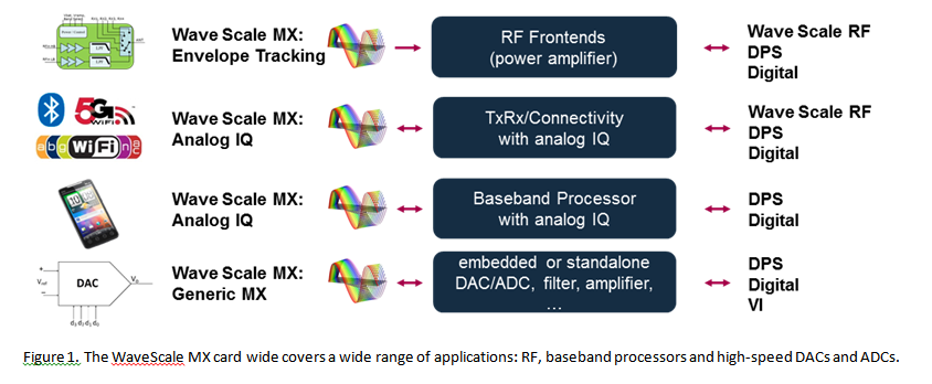
 TAS product family of terahertz analysis systems that enable spectroscopic imaging and measurements; nanotechnology E-beam lithography for nano-patterning and MVM-SEM® for nano-scale measurement; the EM360 dashboard, enabling complete test-floor management and planning; the M6245 and M4871 handlers that boost testing productivity; Advantest’s innovative CloudTesting™ Service for on-demand testing; and specialty products such as the MicroLTE portable test system and SmartBox™, a diagnostic test solution for mobile communication devices from W2BI, Inc., an Advantest Group company.

Advantest technologists were also active in technical sessions during SEMICON West. In the Test Vision 2020 program, Derek Floyd presented his paper on “New ATE Solutions for Upcoming Analog Test,” and Dave Armstrong discussed how “Thermal Testing of Singulated Devices Gets Us Closer to Known-Good Die/Stack.”  During the technical session on Analog and New Frontiers, Advantest’s Takahiro Nakajima spoke on “Test Challenges for Future Automotive 100M/1Gbps Ethernet PHY.”

Read More

Posted in Top Stories

Flexible, Massively Parallel RF Device Testing Is Here

By Adrian Kwan, Business Development Manager, Advantest America

Today’s interconnected world provides great conveniences and many opportunities for staying in touch with family, friends and colleagues – not to mention our physical environment and our own health. Our daily lives are replete with smartphones, tablets, cameras, RFID tags, and wearable/sensor-driven devices – all of which require semiconductor ICs to perform to specification. In the wearables category alone, industry estimates project an annual $5-8 billion demand for ICs to supply this market, driven by requirements for low power, connectivity, sensors, and touch and voice interfaces.

All of these devices are connected through a variety of wireless standards: LTE, LTE-Advanced and LTE-A Pro smartphone standards, as well as LTE-M, WLAN, GPS, ZigBee and Bluetooth. This surfeit of standards creates technological complexities, as these wireless technologies – many of which are enabling the Internet of Things (IoT) – have unique requirements and performance criteria that differ depending upon the application. In addition, while 3G/4G LTE technology currently drives the majority of cellular data traffic and covers the most frequencies, 5G is lurking on the horizon and will bring new production challenges.

Devices based on all of these wireless technologies must be fully tested and characterized before they can be brought to market. This makes flexibility and scalability of automated test equipment (ATE) a fundamental requirement. Advantest is answering this demand with new offerings specifically developed to accommodate the testing demands associated with current and emerging RF chips.

Advantest’s Wave Scale™ generation of channel cards for the V93000 “universal pin” test platform represents a paradigm shift in testing RF and mixed-signal devices, delivering unprecedented levels of parallelism and throughput unmatched by other solutions.  The V93000 Wave Scale RF and V93000 Wave Scale MX cards substantially reduce the cost of test and time to market for RF semiconductors while creating a path for testing future 5G devices.

IMG_2574[7]Current RF testing solutions, which typically require multiple cards plus a separate calibration kit, have employed a fan-out architecture in which subsystem resources are shared. This means that devices with multiple frequency paths are actually tested in serial within the device, rather than in true parallel mission mode testing. It also means that only one RF standard can be tested at a time per site. The V93000 Wave Scale RF condenses four independent RF subsystems into one fully integrated instrument with massive parallelism – as many as 32 ports on each unit, with up 6 units in each system provides the flexibility of up to 192 ports for parallel testing of multiple RF device types. This is enabled via in-site parallelism, in which shared resources are omitted, thus removing the limitations placed on test speedup by other RF test solutions.

Wave Scale RF and corresponding Wave Scale MX cards can simultaneously test multiple standards or multiple paths within each RF device, achieving both in-site parallelism and high multi-site efficiency. Devices can be tested 2-3x faster than with prior solutions – significantly reducing the cost of test. This is a key requirement for OEMs and fabless semiconductor companies needing to get volume RF-enabled devices to market as quickly as possible.

Both Wave Scale RF and Wave Scale MX feature built-in calibration, and both are water-cooled at the pin electronics level to maintain consistent temperature across all pins. The Wave Scale MX high-speed card is optimized for analog IQ baseband applications and testing of high-speed DACs and ADCs. As with Wave Scale RF, Wave Scale MX omits shared resources, delivering parallel, independent operation of all 32 instruments controlled by a hardware sequencer.

Device integration, market segmentation and performance improvements are the inevitable result of consumer demands for more capability, convenience and mobility. Advantest is leading the way for next-generation RF ATE with its new V93000 Wave Scale solutions, designed to simultaneously support the diverse performance and economic needs of new RF device standards.

Find out more:

Read More

Posted in Top Stories

Testing Ultra-Fast Memories…Ultra Fast

By Ken Hanh Lai, Director of Memory Marketing, Memory Business Development

Advanced high-speed test is becoming increasingly important as ultra-fast memory ICs are integrated into a greater number of end products. High-speed memory test systems need to accommodate this trend and offer advanced memory test capabilities for such high-speed ICs. One key category of high-speed memories is GDDR5 (graphics double data rate memory), designed for use in graphics cards, game consoles, and high-performance computational products. These devices include a high-speed parallel data bus that operates at around 8 gigabits per second (Gbps) today and is targeted to go up to 16 Gbps in the future (GDDR5X, GDDR6).

Other fast memory ICs operate using high-speed serial interfaces. Often, a serial bus can be operated at higher overall data rates than a parallel bus because a serial bus inherently has no timing skew or crosstalk. Examples of this include Universal Serial Bus (USB) and PCI Express (PCIe).  The benefits of these implementations include cost-effective, lower-pin-count designs.

These new memory test challenges are being addressed by the new HSM16G, a fully integrated memory test card recently introduced by Advantest (Figure 1). The card extends the high-speed testing capabilities of the company’s V93000 HSM series of testers to native 16 Gbps for at-speed testing of ultra-fast memory ICs. The card provides 32 channels, which are set up as 8 differential receive (RX) and transmit (TX) lines in the 16-Gbps operation mode. Additionally, the card can be switched to two lower-speed operating modes: an HSM8G-compatible operating mode for up to 8-Gbps operation and a 32-channel I/O base mode for up to 1.8-Gbps operation.

HSM 16G Figure 1.  Advantest HSM16G card for ultra-fast-memory test.

The V93000 HSM Series with the HSM16G card provides ultra high-speed memory test capabilities in a cost-effective, small-footprint tester, making it well suited for engineering, design verification, and characterization. Other, less-fast testers have to perform complex multiplexing using lower speed channels  with add-on solutions to reach the speeds needed to test future GDDR5 and other high-speed devices. Because of the subsequent multiplexing, algorithmic pattern generation (APG) is significantly restricted, and only a limited feature set is available for characterization and debugging. The HSM16G card avoids these constraints thanks to its native 16-Gbps speed.

The new card features comprehensive measurement capabilities, including per-pin algorithmic pattern generation to test any kind of fault algorithm and fail bitmap capture. Programmable equalization allows for cable-loss compensation and rise-time control to support the highest signal integrity. A precision per-pin clock with less than 1 picosecond (ps) jitter enables the industry’s most accurate jitter measurements. Further capabilities that set the HSM16G apart are its per-pin-based arbitrary jitter modulation for device characterization and stress test, as well as a set of integrated analysis tools. Key volume-production features include per-pin embedded searches for rapid alignment to the center of the data eye, fast eye measurements to screen for both eye height and eye width, and an integrated time measurement unit (TMU) for accurate jitter measurements.

For memory ICs with serial bus interfaces such as PCIe and Universal Flash Storage (UFS), the HSM16G card offers comprehensive physical layer test (PHY characterization). This enables the card to cover all memory devices with high-speed serial interfaces or high-speed parallel memory buses.

Fully compatible with the V93000 HSM series’ hardware and software, the HSM16G card can be factory installed or retrofit onto a customer’s installed tester base. It enables reuse of existing test programs for HSM testers, with minimal adaptation, letting customers quickly set up the new card and get to work.

Find out more:

Read More