Pages Menu
TwitterRSSFacebook
Categories Menu

Posted in Top Stories

2025 Viewpoint: AI, Device Complexity Will Continue to Drive Packaging and Test Demands

This article is adapted with permission from Semiconductor Digest. The original article can be viewed here.

By Doug Lefever, Representative Director and Group CEO, Advantest Corporation

I believe many of the technology trends that we’ve seen in 2024 will continue through 2025, especially silicon development related to artificial intelligence (AI) and machine learning (ML) applications. Although socioeconomic factors, supply chain issues, and the risk of a global recession will persist, demand for AI should remain strong throughout 2025, spurring major long-term growth in the semiconductor industry. I expect much of this growth will stem from high-performance computing (HPC) products used in data centers, such as GPU/CPUs and DRAM used in high-bandwidth memory (HBM). 

HPC devices are incredibly complex, and their development presents the industry with numerous unique challenges. To increase processing speed and improve performance, engineers are developing chips with more and more transistors – a single data center GPU can contain billions of transistors. Additionally, many manufacturers are employing heterogeneous integration to group multiple ICs together on a single substrate, reducing chip-to-chip communication delays. So, not only are these HPC devices densely packed with transistors, but they also contain various components, all with different needs and processing speeds, packaged together in a single device. This can lead to hot spots and mechanical failures that have the potential to damage the device and render it unusable. Also, power requirements for these devices are increasing exponentially, demanding test and handling equipment with substantial current supplies and advanced thermal control capabilities. 

Most HPC devices are designed for use in data centers running large language models (LLMs), requiring massive computational resources. To run LLMs efficiently, data centers can pool hundreds or even thousands of these AI/ML processors together for long periods of time. If one fails, they have to start the whole process over. This is driving the industry to incorporate more test insertions and added fault coverage in the manufacturing process to ensure higher reliability. Some customers are adding system-level test (SLT) and burn-in (BI) insertions for an added layer of quality assurance. As the demand for AI continues to grow in 2025, we anticipate an increase in the demand for semiconductor testing to support the development of these high-performance devices.

The products used to power today’s AI/ML applications are far more complex than anything our industry has seen before and will only become more complex with the influx of generative AI in consumer products like smartphones and laptops. Advantest is prepared to provide our industry with the test solutions needed to navigate this complexity and drive innovation in 2025.

Read More

Posted in Top Stories

Optimizing Tester Memory Resources with Xtreme Pooling Technology

By Ronald Goerke, Senior Application Consultant, Performance Digital Business Group COE, Advantest

The rapid evolution of semiconductor devices has amplified the demand for advanced automated test equipment (ATE) that can handle increasingly complex test scenarios for logic devices. ATE vector memory is becoming an increasingly valuable commodity as scan-pattern volume soars. Extrapolations based on data from the International Technology Roadmap for Semiconductors (ITRS) indicate that scan data volume will double every three years, and some new data suggests that with the growth of AI products, scan data could begin increasing tenfold over future three-year periods. Furthermore, as parallel and multiplexed scan give way to multi-gigabit high-speed serial I/O (HSIO) scan (as specified in the IEEE 1149.10 standard or in proprietary implementations), devices with fewer pins require even more vector memory behind every single device pin. 

Contending with the data

Key drivers of this data explosion include higher gate counts, new and more intricate fault models, and chiplets as they demand lower DPPM. Consequently, ATE systems are increasingly likely to run out of memory when testing complex devices. Several possible solutions can help to more efficiently use available memory: you can use higher levels of pattern compression, avoid pattern duplication, simplify instructions, or combine patterns to avoid complex operating sequences, for example. If such steps are not sufficient, you can use site memory sharing, which must be enabled on a per-pattern basis, or traditional memory pooling, which occurs automatically, although the user must consider load-board design. In either case, sharing is restricted to one memory pool, which can create bottlenecks for data-intensive scan and functional test and can complicate load-board design.

As an example, Advantest’s Pin Scale 5000 digital card contains eight modules, each with 32 channels and four test processors, providing eight channels per test processor. The eight channels represent one memory pool, and traditional memory pooling can stack all eight channels of memory behind one pin, with fanout supporting up to eight channels for multisite memory sharing (Figure 1). However, with the traditional implementation, a given memory pool in the Pin Scale 5000 cannot extend beyond eight channels, potentially leading to a tradeoff between a costly hardware upgrade and compromising test coverage and efficiency. 

Figure 1. Traditional memory pooling with the Pin Scale 5000 card can stack eight channels behind one pin.

Extending the memory pool

To overcome this limitation and avoid unpleasant tradeoffs, Advantest has introduced the Xtreme Pooling technology with SmarTest release 8.7.2.0, which extends the vector memory pool for the Pin Scale 5000 card beyond eight channels, delivering unmatched flexibility and efficiency and setting a new standard for high-speed, high-data volume test applications. Xtreme Pooling is enabled by Advantest’s proprietary Xtreme Link communication-network technology for ATE systems. 

Xtreme Pooling implementations are possible because a test program usually does not fill the vector-memory pool of all test processors. In Figure 2, moving from left to right, each group of eight vertical bars represents eight channels of memory available for test processors TP2, TP3, and TP4. The dark areas represent memory that the respective test processors utilize, while the lightly shaded areas represent unused memory that could be allocated to other test processors.


Figure 2. Xtreme Pooling makes underutilized memory, indicated by the lightly shaded area of each bar, available to other test processors.

Several naming conventions help to clarify how Xtreme Pooling works:

  • Xtreme Pool refers to all free vector memory.
  • Donor refers to a test processor whose memory can store data that can be executed on other test processors.
  • Recipient refers to a test processor that can execute vector data copied from other test processors.

In addition, a new pattern property describes two memory locations: local (standard, associated with a particular test processor) and remote (in the Xtreme Pool).

Xtreme Pooling allows any test processor on a Pin Scale 5000 card to store vector data in other test processors’ underutilized memory. Xtreme Pooling can serve in HSIO applications with data rates up to 4 Gb/s in multisite configurations as well as in any application with high data volumes.

By enabling memory pooling and sharing across all channels and test processors within a single Pin Scale 5000 card, Xtreme Pooling extends the vector-memory pooling limit from 28 giga-vectors (GV) to 896 GV, as shown by the equations at the bottom right of Figure 3. Xtreme Pooling also increases the vector-memory allocation flexibility to 256 sites.


Figure 3. This Xtreme Pooling example expands the memory pool to 896 GV, as shown in the equations on the bottom right, and provides fanout to 256 sites.

To enable Xtreme Pooling, the user needs to set a flag for those patterns that should be placed in a remote location. While loading the program, the system analyzes the patterns and test program to configure the recipient and donor channels as well as the required buffer sizes. The remote pattern data content is symmetrically distributed to the available donor channels. During test program execution, the remote vector data content required for the execution of a test suite is copied from the donor pools to the recipient buffers (Figure 4). This preload occurs prior to executing a test suite with Xtreme Pooling patterns, and a user can optionally trigger this process early in the test flow as a background operation. After the execution of a test suite, the relevant buffer is freed up for the next preload.


Figure 4. A bind step downloads patterns for donor channels, and a preload step copies content from donors to recipients.

Use cases

Advantest is currently addressing two primary use cases with Xtreme Pooling for high-performance computing and advanced-packaging devices. First, if some scan pins require more memory than is available in a single test processor’s pool, Xtreme Pooling will enable the use of remote memory from low memory pools or additional empty pools, and SmarTest will automatically distribute the vector data to those remote pools. In Figure 5, unused memory in pools 1 and 2 can be allocated to memory pool 3 to provide sufficient vector memory for a single HSIO pin, for example. When a test requests the remote vector data, SmarTest will copy the data to the recipient before execution.


Figure 5. Unused memory from memory pools 1 and 2 can be allocated to memory pool 3.

The second use case involves multi-site test programs with heavy usage of some signals. As in the first case, SmarTest enables the use of memory from low-memory pools or additional empty pools. Compared to traditional memory sharing among sites, this approach does not require all sites needing access to one signal to be in the same pool to take advantage of vector-data sharing because the same vector data from the donor pool (memory pool 1 in Figure 6) can be copied to multiple memory pools (memory pools 2 and 3 in Figure 6) for zero-overhead fanout to multiple sites (two sites in Figure 6). Note that the use cases illustrated in Figures 5 and 6 are not mutually exclusive; both can be applied simultaneously. 

Figure 6. The same vector data from donor pool one can be copied to memory pools 2 and 3 for zero-overhead fanout to two sites.

Load-board considerations

Xtreme Pooling also has implications for the load-board layout. 

For applications requiring multiple cards, it is important to distribute high-usage vectors among the cards. To find the optimal solution, first determine which DUT pins require the most vector memory and calculate the number of Pin Scale 5000 cards required for that DUT. Then, distribute the memory-intensive signals evenly between all available cards. Figure 7 shows 40 high-usage scan signals distributed among four cards, with 10 high-usage signals per card.

Figure 7. High-memory-usage signals are distributed evenly among four cards.

For success when employing Xtreme Pooling, keep in mind that it works only within one Pin Scale 5000 card; it does not work across multiple cards in one system. In addition, a memory pool can be configured as a donor pool or a recipient pool, but not both, and only vectors can be stored in donor pools, while sequencer programs can be stored only in recipient pools. 

Summary

Xtreme Pooling extends vector-memory capacity up to 896 GV per pin by dynamically redistributing unused memory across test processors. The technology enhances memory availability and simplifies load-board design, mitigating the complexities of wiring and signal routing on dense test boards. Moreover, by providing a software-driven solution to overcome memory constraints, Xtreme Pooling supports cost-effective scaling and boosts overall test efficiency with reduced reliance on specialized hardware configurations. Advantest, in collaboration with leading semiconductor companies, has already demonstrated Xtreme Pooling’s value for cutting-edge applications. As data volumes continue to grow exponentially, Xtreme Pooling offers a scalable, cost-effective solution that enhances test versatility, reinforcing Advantest’s position as a leader in the era of increasing device complexity.

Read More

Posted in Top Stories

Early Detection of C-RES Degradation on High-Current Power Planes

By Brent Bullock, Advantest America Inc.

Probe-card or device contactor damage can be dramatic and catastrophic, with yield dropping drastically very quickly. What is not dramatic is the hypothesized slow probe needle or contactor degradation process that might precede catastrophic failure. Such degradation is difficult to detect in the early stages, when probe cards, die, and packages continue to yield normally. A key goal is to detect this degradation as soon as possible to avoid catastrophic damage without incurring yield loss or unnecessary equipment downtime. A related goal is to determine the root-cause scenarios that cause damage to probe needles or contactors.

Measuring contact resistance

One possibility for detecting the onset of probe or contactor degradation is to measure contact resistance (C-RES). This measurement can be accomplished by taking equipment offline, which also allows visual inspection of probe tips. This approach, however, thwarts the goal of minimizing downtime, and it provides limited insight into the root causes of failures—for example, it cannot determine what test sequences were running when a failure occurred. 

Low-current C-RES measurements are valuable, given uniform planarity with clean probe needles. For example, uniform C-RES changes will correlate between I/O pins and large VDD power planes, regardless of pin type (Figure 1, top). However, C-RES can be nonuniform because of particles, needle warpages, device contact defects, or other anomalies affecting a few pins. Unfortunately, low-current measurements cannot detect subtle changes in C-RES for a small percentage of pins isolated within large power planes, rendering nonuniform C-RES issues within large VDD planes unobservable on I/O pins (Figure 1, center). This limitation can be overcome by improving measurement granularity, taking measurements at higher current levels, or combinations of the two.

Figure 1. Probes can exhibit uniform (top) or nonuniform (center) planarity, and sub-gang measurements (bottom) can provide adequate resolution to detect anomalies in the latter.

Sub-gang measurements

One approach to improving C-RES measurements despite nonuniform contact problems is to take advantage of the fact that a VDD power plane is likely to be powered by multiple power-supply channels. The multiple channels allow sub-gang per-channel measurements that can provide sufficient granularity to detect C-RES variances with adequate resolution (Figure 1, bottom). For example, Advantest’s EXA Scale generation of instruments for the V93000 platform includes power supplies, digital comparators, and data converters (Table 1) that can discern C-RES variations between channels.

Table 1. Exascale instrument capabilities and specifications

EXA Scale instruments can determine C-RES by measuring the voltage drop (vDrop) across the probe head for a given measurement current. vDrop can be measured and recorded at a specific point in time or averaged over multiple points in time. This approach may require additional test time, and, similar to off-line measurements, it provides limited insight into the root causes of failures.

Monitoring vDrop

A better approach involves the monitoring of vDrop using continuous ADC sampling and the triggering of an alarm when significant C-RES anomalies occur. This approach has the added advantage of pinpointing what test sequences were executing during significant C-RES changes, thereby facilitating root-cause analysis. Figure 2 shows the XHC32 ultra-high-current power supply configured to provide such continuous monitoring of the C-RES values on both the VDD and VSS sides of the die. This approach requires an extended sense line, which must be added during DUT board design, in addition to the primary sense line.

Figure 2. An XHC32 extended sense line monitors the delta value relative to the primary sense line.

Advantest’s SmarTest ATE software includes a feature that facilitates the programming of the extended monitoring and alarm functions in either interactive or API modes. Figure 3 shows results with per-channel ganging granularity, initiated by checking the perPogo box in the instrument view (left). Data for each channel is shown on the right, with the highlighted channel showing a significant anomaly in measured current. To further control the ganging granularity, Advantest offers a capability called Ganged on the Fly dynamic master-channel switching, which is useful for changing the master sense line when the IR drop across a power plane varies with test content. The capability supports unique signal names for desired master-channel scenarios.

Figure 3. Checking the perPogo box in the instrument view (left) enables the display of per-channel results (right).

Measurement results and comparisons

Figure 4 shows actual waveform results, with the extended vDrop profile shown in blue and the current shown in yellow. Extended vDrop scales with the current flow, with capacitor charge/discharge cycles inducing transient variations. 

Figure 4. The extended vDrop value (blue) scales with current (yellow), with capacitor charge/discharge cycles inducing transients.

Figure 5 shows the extended vDrop and current values shown in Figure 4 converted to power (brown) and C-RES (blue) values, with C-RES impacted by device contacts as well as the probes. The conversion is part of Advantest’s new contact rating feature, which eliminates the issue of having to adjust for power, reducing engineering workload.

Figure 5. The brown and blue traces represent power and C-RES, respectively, derived from the voltage and current traces in Figure 4.

Figure 6 shows vDrop measurement trial data for two equipment setups A and B, which each have induced variations in the equipment and known variances in DUT contact quality. Measurements were taken for three separate tests, with each test performed four times, once for each of the two setups using the lower power Core Supply A and once for each of the two setups using the higher power Core Supply B. 

As shown in the figure, tests run on each setup using the low-power Core Supply A yield very similar results. For example, the measurements at the left of the Core Supply A results show that test 264 run on Equipment Setup A (Series 1) and the same test run on Equipment Setup B (Series 2) yield nearly identical measurements, making it difficult to draw inferences about C-RES variations. In contrast, the results for the same test run on the same two setups using the higher power Core Supply B are clearly distinguishable, demonstrating improved capability for vDrop measurements, and hence C-RES measurements, when utilizing currents that represent a higher percentage of total CCC.

Figure 6. Measurements taken with the lower power Core Supply A (left) and the higher power Core Supply B (right) show that the higher power supply provides improved capability for distinguishing C-RES variations.

Summary

Extended vDrop measurements can detect test-cell variations but have limited potential for isolating root causes of probe failures. In contrast, extended vDrop monitoring with alarm functionality is effective at detecting C-RES degradation, and because the monitoring is continuous, it is also effective in determining the root causes of the degradation—for example, test program sequences that may inadvertently apply too much current.

The implementation of vDrop monitoring requires planning because C-RES measurement or monitoring is not possible without proper routing, and the required extended sense lines must be designed into the DUT board. For the best results, retain the primary sense lines in the same location used for previous designs and add the extended sense lines on the opposite side of the die or contactor. Advantest offers the instruments and software necessary to implement extended vDrop monitoring and is performing additional work to automate the process of setting adaptive current clamp and vDrop alarm limit values.

Read More

Posted in Top Stories

AI Semiconductors Require an Integrated Test Solution

By GO SEMI & BEYOND Staff

The rapid proliferation of generative pre-trained transformers based on large language models (LLMs) is driving growth in the market for chips that can run the LLMs and other artificial intelligence (AI) and machine learning (ML) applications. Several types of chips hold promise for accelerating AI computing. Graphical processing units (GPUs) have proven to be capable solutions for the server/cloud environment, although work is underway on dedicated AI chips that could offer higher efficiencies. Edge applications will require lower-power devices, such as neuromorphic chips, which mimic neural network behavior. Personal computers are also gaining AI capabilities as chipsets appear to accelerate AI program execution without requiring cloud resources.

AI chip market

Research firms see a booming market for these AI-capable chips, although the exact numbers remain unclear because of the variety of classes of the devices. Mordor Intelligence forecasts that the market for GPUs will grow from about $65.3 billion in 2024 to $274.2 billion in 2029, driven by both graphics and AI applications. For its part, Gartner forecasts that worldwide AI chip revenue will increase from $53.4 billion in 2023 to $119.4 billion in 2027. Future Market Insights takes a longer look and forecasts that the AI chipset market will increase from $27.6 billion in 2024 to $287 billion in 2034—a CAGR of 26.4%. Deloitte puts the market for specialized chips optimized for generative AI at more than $50 billion in 2024, representing two-thirds of all AI chip sales during the year.Market.us surveys the complete global AI chip market, including GPUs, and estimates it is growing at a CAGR of 31.2% and reaching $341 billion in 2033.

Finally, as AI comes to the home and business desktop, personal computers will increasingly include dedicated chipsets that can accelerate AI computing, executing AI applications without requiring cloud connectivity. Canalys predicts that 60% of PCs shipped in 2027 will be “AI-capable,” up from 10% in 2023.

AI chip characteristics and test challenges 

The diverse classes of chips applicable to AI computing present unique test challenges, but several are common to most of them. For example, increases in device complexity are causing an explosion in scan-pattern depth, with pattern depths moving from what used to be a doubling every three years toward increasing tenfold every three years. Such growth necessitates new ATE technologies as well as the use of more efficient test data distribution schemes inside the device for higher throughput and parallel test of multiple cores.

The test flow for AI-enabled chips remains similar to that for traditional devices. Key stages in the flow include post-silicon validation, wafer acceptance test, wafer sort, final test, burn-in, and system-level test (SLT).

However, test-flow stages must become dynamically adaptable with real-time decision-making to minimize the cost of the test (COT), maximize yield, and facilitate dynamic failure analysis. In addition, test must occur in accordance with specific application requirements because scan testing exhaustively is becoming too expensive. Consequently, functional test content is moving forward in the flow in order to focus the valuable test time on the best parts. Additionally, binning must move from the performance-based approach of traditional test to an application-based approach that facilitates die matching (harvesting and smart pairing).

The dynamically adaptable test flow requires the seamless sharing of data across multiple test insertions and throughout the manufacturing process. It is also necessary to correlate behavior across insertions—to predict from a wafer-test result what will happen at future insertions, for example, and to identify defects before packaging.

Products and Services for AI chip test

Advantest offers a full lineup of test solutions for AI-capable chips that perform high-quality, cost-effective tests at high throughput. These platforms feature a module-based architecture that enables flexible reconfiguration of test modules to meet the ever-expanding list of test methods and applications.

In addition to the test platforms, Advantest offers associated equipment ranging from die-level handlers and thermal controllers to test-interface boards. In the handler and thermal-control category, Advantest provides the HA1200 die-level handler to support the test of singulated or partially assembled die. Equipped with Advantest’s ATC advanced thermal control option, the HA1200 enables known-good-die (KGD) testing of high-power, high-performance AI-capable devices within a thermal environment similar to their final assembly location. Testing in this fashion helps ensure true KGD for parts shipped in die form, chiplets, and large AI components that use back-side power delivery.

The company also offers an ATC 2kW solution for its M487x handler series to provide advanced thermal control at final test. Rounding out the hardware offerings from Advantest are high-performance DUT boards, test sockets, and thermal-control units, which accommodate very large form factor devices, including ones with coaxial electrical interfaces.

Advantest SLT and burn-in systems also provide a variety of thermal options to accommodate these large packages and high-power devices. These SLT thermal solutions include but are not limited to, active cooling and heating with fast dynamic response to maintain setpoints without overheating the DUT.

To handle the compute-intensive aspects of chip production and test, Advantest offers Advantest Cloud Services (ACS), which provide data management and analytics to pull together data from across the value chain. Included in ACS is Advantest’s ACS Real-Time Data Infrastructure (ACS RTDI) platform, which collects, analyzes, stores, and monitors semiconductor test data in a True Zero Trust security environment to enable customers to convert insights into actionable steps while protecting IP. In addition, the company’s ACS Edge platform can work in conjunction with Advantest’s platforms to handle computationally intensive workloads locally without loading down the test program or requiring cloud intervention. This addresses the growing industry need to run advanced, complex analytics at multiple test insertions while achieving very low and predictable latency.

Scan test

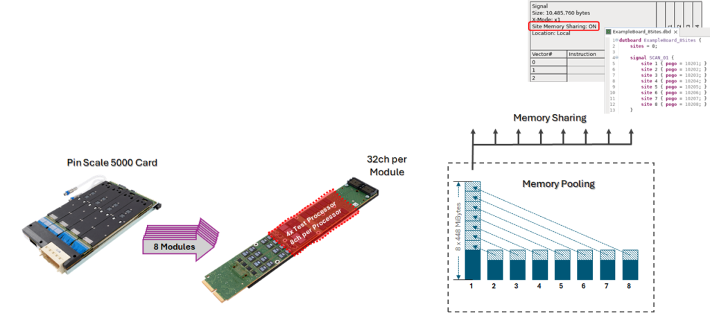
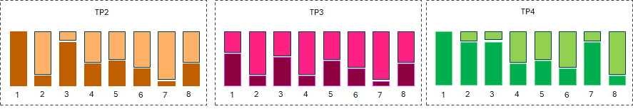
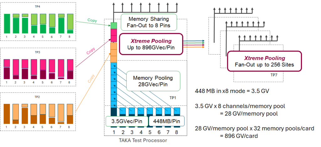
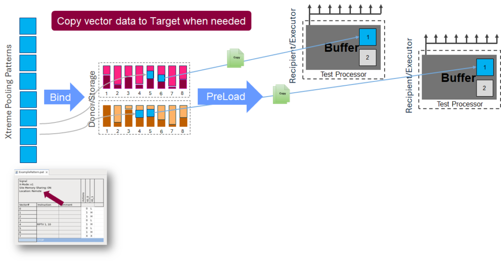
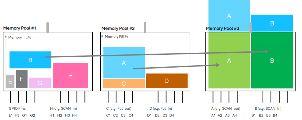
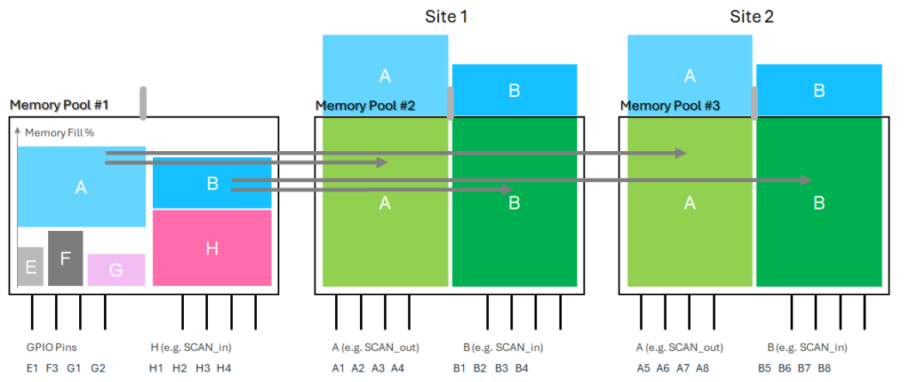
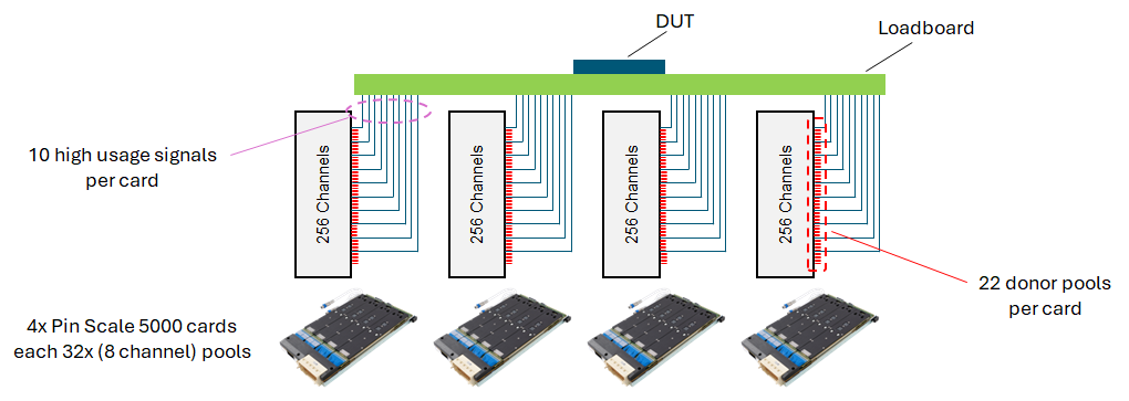
For scan test, the tester must efficiently move scan data in and out of the DUT. Test patterns must be deployed at the KGD testing step as well as at the final test of the complete heterogeneously integrated device. To accommodate tenfold pattern depth increases, testers require much greater memory depth. To meet this requirement, Advantest offers the Pin Scale 5000, which has multiple giga vectors per pin at up to 5 Gb/s.

Compression and memory pooling can scale this capacity significantly, either per pin or across multiple pins.

Some devices already require terabits of scan-pattern test data. Depending on the scan architecture, the available I/O speed, and the number of I/Os available for scan test, it can take many minutes to run a comprehensive scan pattern set on a very large device, which leads to high test cost and low throughput. As an alternative, a device’s native PCIe interface running at 16 Gb/s (with future versions moving to 32 Gb/s and 64 Gb/s) can also transport scan test data if the device-internal DFT supports it. To enable the use of PCIe or other serial interfaces, Advantest offers the Link Scale digital channel cards for the V93000 platform that enable software-based functional testing and PCIe (or USB) scan testing. Coupled with the latest generation of on-die scan data distribution networks, Link Scale can provide an order of magnitude faster pattern execution compared to traditional approaches. Alternatively, Advantest’s SLT and burn-in systems can utilize the same device-internal DFT and our controllers’ PCIe or USB interfaces to execute the same SCAN patterns that were generated for use on the V93000 Link Scale solutions. SLT and burn-in systems typically are less expensive per test site but run for much longer durations.

Power requirements 

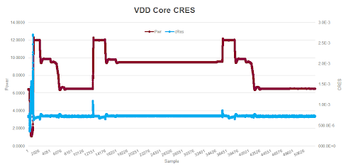
The tester must also deliver sufficient power to the DUT while preventing overheating. Some devices are already drawing over 1,500 A, with future plans for 2,500 A and more, so controllability of the power resources is critical, requiring precise regulation, fast clamping capability, and in-line monitoring of contact resistance. In addition, supply voltages are being reduced from 1 V down to 750 mV, 600 mV, and even 500 mV. Each voltage drop requires higher accuracy. Power supplies must also be simple and flexible, enabling system configuration without buying more resources than needed.

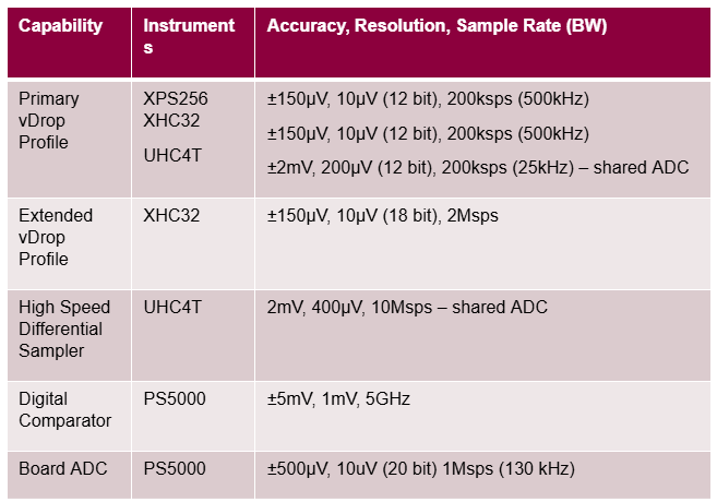
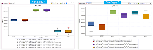
To meet test power-supply requirements, Advantest now offers the XHC32 high current power supply for the V93000, which delivers up to 640 A per card and is an ideal complement to the widely used XPS256 universal power supply. Both cards feature digital regulation, fast clamp response, extended profiling capabilities, and state-of-the-art protection features for probe cards and sockets. In combination, they serve the needs of power-hungry performance digital devices for years to come. For our SLT and burn-in test cells, a similar power is available to each DUT in a highly parallel environment.

Scan and power requirements, taken together, have implications for multisite test as DUT pin counts vary. Scan port width may vary from tens of pins to hundreds of pins, and power requirements are constantly increasing. Bandwidth requirements for test data transmission greatly increase in parallel. Very large devices combining multiple dies in one package are also becoming increasingly prominent, especially in the HPC segment. As these chips have large numbers of I/Os, real estate on existing DUT boards is not always sufficient to accommodate all the external components required for test, especially in multi-site setups. The new DUT interface DUO available on the V93000 helps with this by significantly increasing the available space for large DUT interface boards while maintaining compatibility with existing DUT boards.

Boot-up and system-like test

In addition to scan and functional test, the tester must confirm that the chip meets its intended requirements for AI applications, such as object recognition. This level of testing requires DUT boot-up and execution of software on the DUT during the test insertion, which is typically performed during SLT. Interfaces such as PCIe are suitable not only for scan but also for the exchange of large amounts of data that would enable a chip to run a convolutional neural network or similar application. Boot-up sequences and interfaces such as PCIe can present fundamental problems that, if found only at SLT, impose significant time and cost issues for parts destined for heterogeneous integration.

To avoid these issues and to shift the boot-up test left, Advantest offers system-like test™ technology, which can help shift boot and other SLT content to wafer probe. Link Scale can alternatively act as a source of data, providing a data array for an AI processor.

Machine-learning driven test

And finally, Advantest is also leveraging ML to test ML-capable devices. The company has demonstrated test time and cost reduction using intelligent prediction from ML models. Customers with strong in-house data-science teams can develop similar models and run them on Advantest’s infrastructure. Advantest is continuously investigating AI-based methodologies to support its customers.

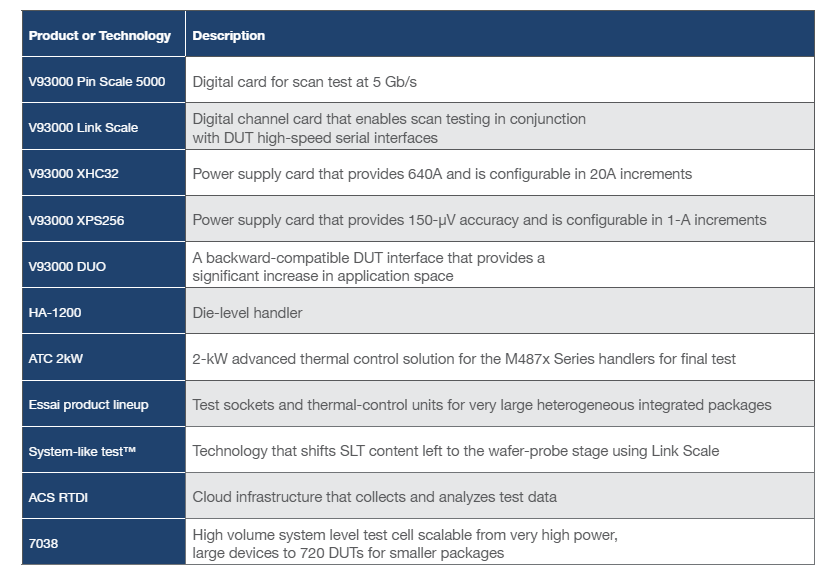
Table 1. Advantest products and technologies for AI-enabled chip test

Conclusion

As we step into the AI-driven future, the complexity of testing AI-enabled chips intensifies, marked by significant increases in test-data volumes and challenges related to heterogeneous packages with restricted access. Advantest is at the forefront of addressing these challenges with its robust portfolio (Table 1) of cutting-edge test hardware and sophisticated cloud-based services. Leading this transformative era, Advantest ensures its customers consistently remain on the leading edge of technology. By not only meeting today’s stringent demands for AI chip testing but also anticipating future needs, Advantest positions its partners for success. As AI reshapes industries and expands the horizons of possibility, facing the future of technology together with Advantest ensures your technology is always ahead and fully equipped to leverage the immense potential of the AI era.

Read More

Posted in Top Stories

Advantest Celebrates 25th Anniversary of Industry-Leading V93000 SoC Test Platform


Earlier this year, Advantest celebrated the 25th anniversary of its flagship V93000 system-on-chip (SoC) test platform. The V93000 revolutionized the semiconductor test industry with its single scalable platform approach, enabled by its test processor-per-pin architecture, which has endured over four generations. As a testament to this endurance, the very first V93000 system installed is still in use at the customer site in Italy, alongside several recently purchased fourth-generation V93000 EXA Scale testers.

 Upon its introduction in July 1999, the V93000 “quickly became a true landmark, as most top-end SoC testers after it would copy the system’s architecture for many years to come,” according to the Chip History Center. Since adding the V93000 to its portfolio when Advantest acquired Verigy in 2011, Advantest engineers have continually enhanced and expanded the V93000 scalable platform to offer a wide range of compatible tester configurations – from small-footprint engineering systems to very high-pin-count wafer sort and final test systems for high-volume manufacturing. The V93000 provides the industry’s broadest application coverage, including high-performance computing, artificial intelligence, RF, automotive and industrial, to name a few. The accompanying chart enumerates Advantest’s many advancements to the V93000 test platform over the years.

TechInsights Vice Chair and Senior Fellow G. Dan Hutcheson has long followed Advantest and the trajectory of the V93000 platform. “The V93000’s long life is an icon for the virtuous cycle that can be created when a team of tool designers thinks beyond the challenges of the day to develop an architecture that can evolve to address as-yet-unknown future challenges. In the case of the V93000, its long life has benefited both Advantest and its customers,” Hutcheson observed. Advantest has been named to TechInsights’ annual 10 BEST list for each of the 36 years that the market intelligence firm’s Customer Satisfaction Survey has been in existence.

“Technology evolves at a lightning pace, so reaching the quarter-century mark is a milestone achievement that underscores the value of our single, scalable platform approach,” said Juergen Serrer, senior executive officer and chief technology officer, Advantest. “Partnering with our customers to stay ahead of technology trends has enabled us to ensure that the V93000 platform stands ready, with state-of-the-art capabilities, to accommodate today’s and tomorrow’s test challenges. We look forward to what the next 25 years have in store.” 

Click to enlarge

Read More

Posted in Top Stories

Advantest Ranked Third in Forbes JAPAN’s “100 Great Companies” Stakeholder Capitalism Ranking

By GO SEMI & Beyond Staff

In October, Advantest announced that it had earned third place in the stakeholder capitalism ranking published as a part of the “100 Great Companies” special feature in Forbes JAPAN, the Japanese edition of the global business magazine Forbes (December 2024 issue, published on October 24).

The “100 Great Companies” ranking was independently calculated by Forbes JAPAN with the cooperation of Sustainable Lab, which collected and analyzed sustainability-related data in five categories: natural capital, employees, shareholders, suppliers/communities, and customers/consumers. The analysis covered 1,644 companies on the Tokyo Stock Exchange Prime Market. Companies were scored on indicators in each of these categories, based on a relative evaluation of each industry, and the final score for each company was calculated by weighing the scores compared to the rest of the industry. 

Advantest defines sustainability as meeting the needs of the present without compromising the needs of future generations.

Advantest aims to be the most trusted and valued test solutions company in the semiconductor value chain. To achieve this vision, the company is committed to meeting the expectations and needs of its global stakeholders. Advantest strives to provide a balanced mix of economic and social values, contributing to global sustainable development while enhancing its corporate value in the medium to long term.

Read More