Pages Menu
Categories Menu

Posted in Top Stories

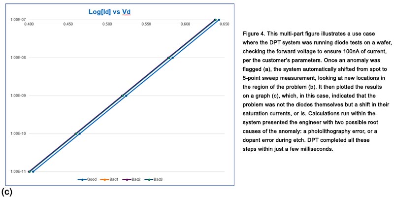
SLT Enables Test Content to Shift Right to Optimize Test Efficiency and Part Quality

By Dave Armstrong and Davette Berry, Directors of Business Development, and Craig Snyder, Business Development Manager

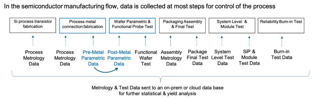
Increasing device complexity and the continuing drive for higher levels of quality are fostering a reconsideration of test strategies. To be effective, test engineers must choose how to optimally deploy test content, from wafer probing to system-level test (SLT). A March 2019 TestConX presentation1 outlines how test content is typically allocated—for example, final test performs structural and functional tests, parametric measurements, and performance binning; burn-in screens for early-life failures; and SLT looks for mission-mode failures resulting from hardware and software interactions. For cost balancing, though, it might be preferable to transfer a test step that has traditionally been performed at final package test, for example, upstream toward wafer test or downstream to SLT. At Advantest, we call the upstream transfer “shift left” and the downstream transfer “shift right” (Figure 1).

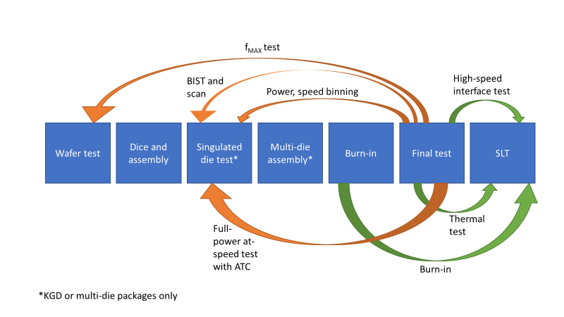
Figure 1. The test flow from wafer probing to SLT offers opportunities to shift test content right or left to optimize test efficiency and part quality.

Shift left overview

A January-February article2 in Chip Scale Review describes the shift left process, which is particularly applicable to the integration of heterogeneous known-good die (KGD). For KGD test, it is advantageous to shift test content left from final test toward wafer test or to a singulated-die test stage, where you can perform full-power active-thermal-control (ATC) testing at speed. For KGD, a shift left strategy of more testing sooner reduces the number of good die scrapped because of one bad part in a multi-die assembly, ultimately leading to lower costs and more profit.

SLT overview

Alternatively, other applications can benefit from a shift right strategy, in which some test steps are transferred from final test and burn-in toward SLT, especially as SLT becomes more pervasive in manufacturing test.

SLT mimics in a manufacturing test environment the real-world operating conditions of the device under test, as described in a September 2020 GO SEMI & BEYOND article. In SLT, the device under test interacts with its mission-mode software and communicates with peripheral devices including power-management ICs (PMICs), DRAMs, and high-speed interfaces including USB or PCIe gen 4. Originally focused primarily on the memory and storage market during early silicon bring-up, SLT has expanded to include test of high-end processors and systems on chips (SoCs) used in computing, mobile, and automotive markets as well.

In addition to expanding to more markets, SLT is increasingly being applied to 100% of manufactured parts—not just samples. 100% SLT opens the door for a shift right of many test functions from final test to an enhanced SLT stage. This shift may also result in a lower overall cost of test.

High-speed interface test

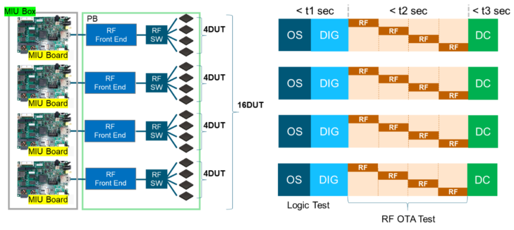
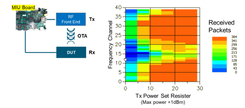
One opportunity for the shift right of test content from final test to enhanced SLT involves connectivity and the test of high-speed I/O, but high-speed I/O tests bring about key challenges. In mission mode, a device will likely be soldered to a printed-circuit board close to its peripheral circuitry or inserted into an OEM socket on a computer motherboard. Neither is possible in the manufacturing test environment of SLT.

In SLT, connectivity and signal degradation problems—not defective devices—cause significant first-pass yield problems, seriously compromising throughput due to retest.

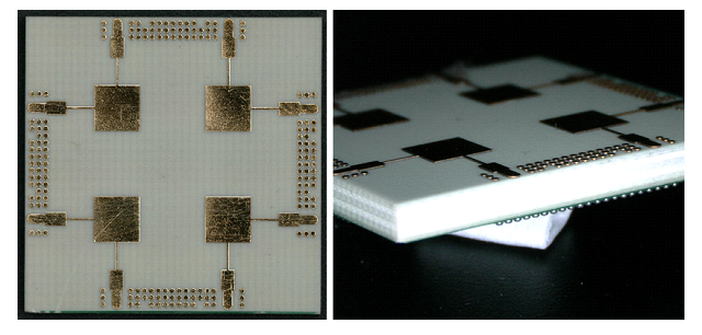
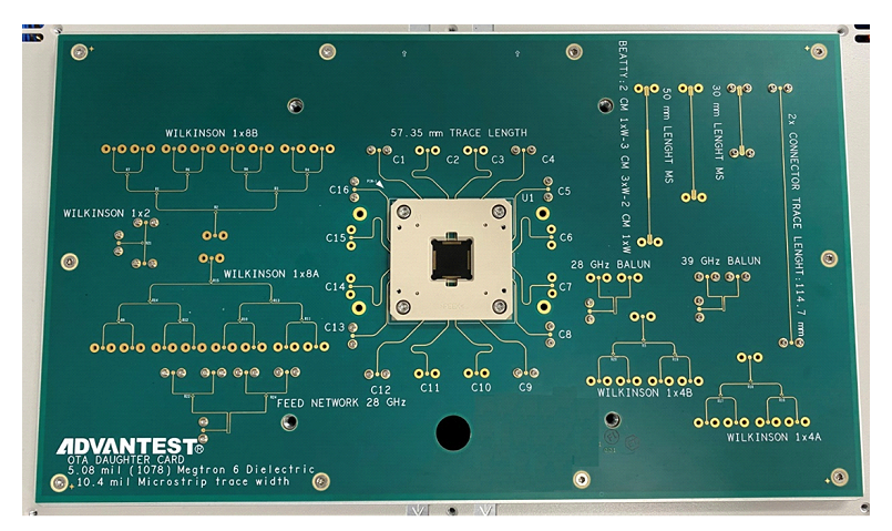
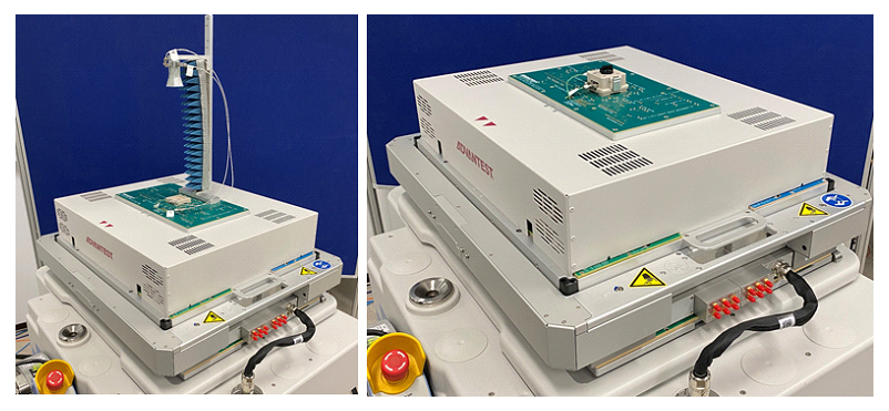
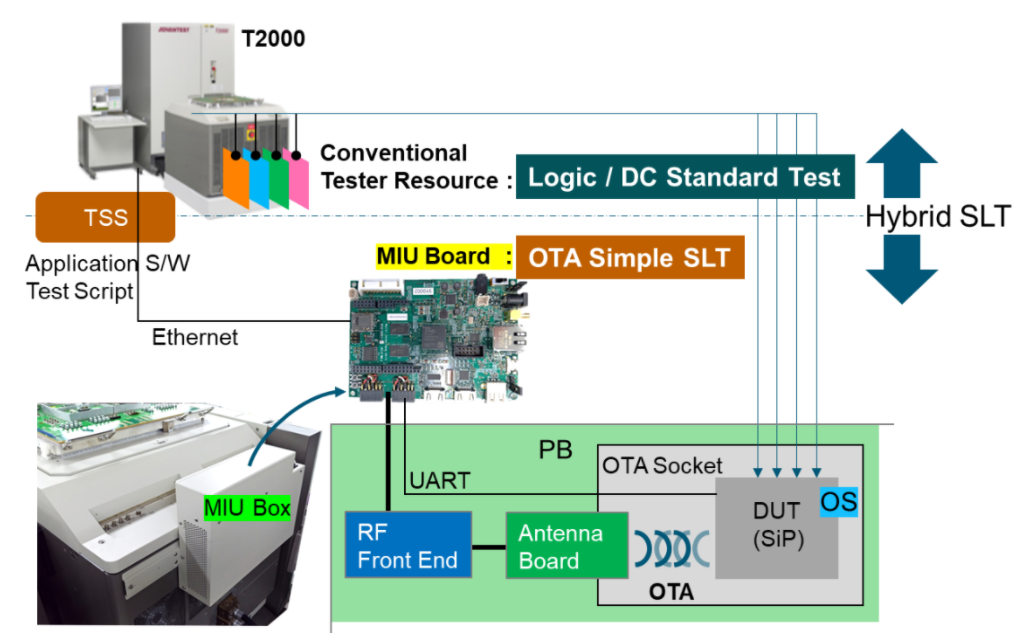
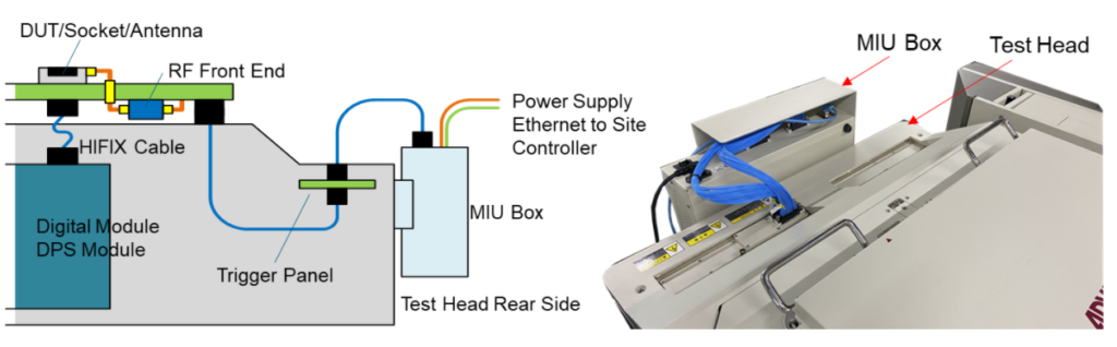
What’s needed is a high-performance, high-durability test socket for use in SLT that provides an optimized, tuned interconnect between the chip under test and its peripheral circuitry. To that end, Advantest in January 2020 acquired Essai, a supplier of semiconductor final-test and SLT test sockets (Figure 2) and thermal-control units. Essai possesses the expertise to design and manufacture the sockets with ever smaller pitches and ever higher electrical and thermal performance to address the final-test and SLT needs for successive generations of chips. These sockets permit at-speed test of high-speed interfaces at SLT, thereby enabling full-speed system level testing.


Figure 2. A test socket suitable for SLT provides mechanical durability while supporting an optimized signal path from the device under test to its peripheral components.

In addition, the socketed SLT motherboard enables a more native environment configuration for the device under test and better represents real-world conditions than does a typical ATE final test insertion, where propagation delays related to the path from device through the socket and load board and finally to the instrument must be taken into account.

Thermal test

Almost all of Advantest’s SLT customers are testing device behaviors at different temperatures at some point in the test flow, and most, if not all, of these tests can be shifted right to the SLT environment. 

An example in the automotive industry is the cold-boot requirement to ensure that vehicle electronics will boot up on an Alaskan winter morning. 

SLT can exercise a device at high temperatures, too. Many devices have temperature sensors, which may trigger a processor at a certain temperature to communicate with a PMIC to initiate a low-power operating mode until the temperature returns to normal.

Testing across temperature ranges presents its own challenges. For example, when you subject the device to different temperatures you are also subjecting the interconnect to different temperatures, leading to potential failures due to expansion and contraction. One solution is to get the device to temperature while leaving the rest of the SLT environment at as neutral a temperature as possible. Further, with heterogeneous integration, a substrate which may be as large as 100 mm on a side may accommodate multiple die, each with its own thermal response and challenge. Such a package might require topside contact by a thermal interposer that maintains temperature setpoints within different zones, all within that same package.

Burn-in

Finally, burn-in is a common test insertion for both automotive and high-performance compute devices. SLT test times extend from less than a minute to tens of minutes, and burn-in times extend from tens of minutes to hours. Given that the burn-in and SLT test insertions require some common thermal stress infrastructure, Advantest can enable the automation of combining SLT and burn-in in a common test cell. With some customers exploring high-speed I/O test during burn-in, burn-in can offer another opportunity to shift test content right.

Conclusion

Ultimately, in addition to its role mimicking the device under test’s mission mode, SLT is an opportunity to shift test content right. What it is not is an opportunity to completely replace other test steps. There will always be a need for final test, covering at a minimum short/open test to find assembly defects and performing multi-die communications checks and/or parametric measurements. On the other hand, the SLT test often includes creative interconnect solutions to high-speed memory, which require a test environment that would be impossible on an ATE system.

Committing to SLT for 100% of devices is a big step for companies to take, but once they do so they find that they can simplify final test by reducing test redundancy while continuing to ensure, and potentially enhance, the level of quality. Advantest serves the entire semiconductor manufacturing test space, from wafer probe to SLT. Advantest engineers stand ready to work with customers to determine the optimum deployment of test resources for their specific applications.

References

  1. Berry, Davette, et al., “Holistic approach to test coverage across Final Test, Burn In, and System Level Test,” TestConX, Mesa, AZ, March 3-6, 2019.
    https://www.testconx.org/premium/wp-content/uploads/2019/TestConX20193ap2_5612.pdf
  1. Armstrong, Dave, “Heterogeneous integration prompts test content to ‘shift left,’” Chip Scale Review, January-February 2021, p. 7.
    https://chipscalereview.com/wp-content/uploads/2021/01/ChipScale_Jan-Feb_2021-digital.pdf
  2. Pizza, Fabio, “System-Level Test Methodologies Take Center Stage,” GO SEMI & BEYOND, September 27, 2020.
    http://www.gosemiandbeyond.com/system-level-test-methodologies-take-center-stage/
Read More

Posted in Top Stories

Driving Toward Predictive Analytics with Dynamic Parametric Test

By Alan Hart, Senior Director, Applied Research, Technology & Venture, Advantest America, Inc.

The foundation of parametric test within semiconductor manufacturing is its usefulness in determining that wafers have been fabricated properly. Foundries use parametric test results to help verify that wafers can be delivered to a customer. For IDMs, the test determines whether the wafers can be sent on for sorting. Usually inserted into the semiconductor manufacturing flow during wafer fabrication at both the pre- and post-metal phases (as shown in Figure 1), parametric test has traditionally been used to check both transistor fabrication and metal layer interconnection, providing inputs to statistical process control (SPC) tools.


Figure 1. In the manufacturing flow, parametric test is typically inserted pre- and post-metallization, as indicated in blue above.

Measured data generated from the parametric tests is assessed and entered into a database, generating a report for an engineer to review. If an anomaly is highlighted, the engineer then orders the lot to be called back for retesting. This process typically takes a day or two, adding to the length and cost of the manufacturing cycle.

Dynamic parametric test (DPT), on the other hand, removes this review/retest loop by triggering immediate action upon measurement of an anomalous data point, based on the user’s predetermined parameters. This action takes place instantaneously, while the wafer is still on the tester – no reprogramming is required. Essentially, DPT elaborates on SPC techniques to establish these triggers, automating a process that, previously, would have required human intervention.

DPT drivers

The primary driver for implementing DPT techniques is the increasingly tight limitations created by shrinking process nodes. Today, 7nm and 5nm devices are in development (and the first 2nm process was recently announced). This translates to fabrication of leading-edge chips that comprise billions of transistors, whose features are separated by just a handful of silicon molecules. Testing billions of transistors individually is impractical, making parametric test vital for capturing statistics that reveal how the process went and help predict how well the circuit will perform. As devices get smaller and smaller, it becomes increasingly challenging to capture enough statistics to yield meaningful results, thus a greater volume of parametric tests are being applied in the assessment of wafer process quality.

DPT accelerates time-to-problem-solving, and hence, time-to-market, by enabling the parametric test system to instantly initiate data exploration based on customer-defined programming. By affording a deeper understanding of parametric deviations, it allows the user to program detailed characterizations for key devices, and to execute custom test flows based on real-time statistics or other user-defined criteria. As noted earlier, it adds automation to the engineering function – in essence, creating virtual engineering staff that can immediately analyze and debug unexpected results, or optimize test flow for tester utilization.

Advantest’s approach to DPT

Traditional parametric test looks at historical data to see what happened (descriptive analytics). Today, the process is evolving to capture additional data, allowing us to understand why it happened (diagnostic analytics). Going forward, the data will be correlated with future test results, enabling us to predict what will happen (predictive analytics). Predictive analytics, a key objective of Industry 4.0, enables corrective actions earlier in the manufacturing flow, as well as faster extraction of potential root-causes of deviations. Thus, by beginning to connect all the manufacturing steps shown in Figure 1, we can help wafer fabs and foundries begin to reap downstream benefits.

The goal is to be able to understand not only how well the circuit will yield at functional test, but also to predict its reliability when in use in its final application. For example, having one’s mobile phone fail is frustrating, but if it fails when you’re in your car and you need the GPS, or an emergency situation arises and you can’t call for help, the result could be disastrous.

Advantest’s Dynamic Parametric Test (DPT) software is a data-analytics enhancement to the V93000 SMU8 parametric test system, built on PDF Exensio® software from PDF Solutions. Together, Advantest and PDF Solutions have built a focused solution for parametric test that programs human decisions and actions into the tester to add real-time intelligence into the parametric test cell. Users implement DPT to immediately apply modified testing, both test algorithms and die map topology, allowing them to gain greater insight into the causes of unexpected results and to improve the efficiency of the test cell.

Figure 2 illustrates how the two systems work together. The DPT solution includes modifications to both the V93000 SMU8 system software and the Exensio data analytics platform. The solution is integrated into the V93000 SMU8 and into the Exensio server that manages the rules engine. Using customer-created rules, the software evaluates the incoming data from the tester, determines any necessary modifications to the test flow and/or test algorithms, and communicates them back to the tester, which then executes the new recipe. All of this happens instantly, in real time.


Figure 2. The Advantest V93000 Dynamic Parametric Test (DPT) system powered by PDF Exensio® DPT. The V93000 measures data and, via the event data log (EDL) stream, sends it to the Exensio software, which evaluates the data and immediately transmits any adaptive actions back to the test system to run the revised recipe.

No pre-programmed instructions are included in the DPT solution. The customer defines rules and models based on their own historical data and manufacturing requirements, which the system uses to look for anomalies and automatically trigger appropriate actions as the tests are run. The system identifies three basic types of triggers:

  • A value that deviates from historical results;
  • A statistical computation based on historical results from wafers/lots/time; or
  • Statistical trends based on historical results from wafers/lots/time.

The rules that define these triggers and their parameters are set up through a simple user interface, using test algorithms already available in the customer’s test library, and are applied either at the end of the die location test or the end of the wafer test (see Figure 3).


Figure 3. The DPT solution can apply the rules engine at the end of a die-location test or at the end of a wafer test. New data in the modified test flow is automatically collected, without requiring wafer reloading or engineering review.

Real-world example

The ways in which the system can be deployed are limited only by customer needs. As an example, Figure 4 shows a use case involving diode test, checking the forward voltage (Vd) necessary for a 100nA of current to flow through the diode. The spot measurements are distributed across the wafer, as a representative sample provides a good indication of how the entire wafer behaves. When a bad data point is discovered, the system might automatically switch from a spot measurement to a sweep measurement, adding more die locations, to determine whether the cause is a device point defect or a general fabrication problem.

In Figure 4a, the DPT run flagged an outlier device that returned an out-of-spec result. As Figure 4b illustrates, this then automatically triggered a deeper, five-point sweep measurement around the location of the faulty diode, which revealed further outliers in that region. Figure 4c condenses the sweep results, plotting the sweeps to determine what caused the two parallel lines to appear. In this case, the slope shows normal diode behavior, with no device leakage. The problem is thus determined to be a problem with the bad diodes’ saturation current (Is).

The system’s further calculations reveal that Is is only modified by p-n junction area (via photolithography) or by dopant density in the anode or cathode. Knowing the potential contributors of the saturation current are physical area and impurity concentration leads to two different potential root-causes. The engineer can then look at the topological pattern, which, in this case, suggests that the problem was in either a photolithographic or etch step, likely from a single multi-die reticle exposure. Thus, in less than a second of automatic additional testing, DPT has provided the engineer with an augmented data set for quick problem resolution.

The system can detect virtually any type of problem created during the manufacturing process, including back-end probe testing. On most parametric test floors, continuity test failures due to failing probe contact are not uncommon. When a continuity test fails, DPT performs further tests to determine if the problem is actually a defective die location or a probe needle that needs to be cleaned or repaired.

Once DPT validates that previously good die are now failing, it automatically performs a wafer probe card clean/polish step. It then can explore a wider topological region, automatically adding die locations to determine where the continuity problem occurred. If the error was caused by a dirty probe needle, which is often the case, retesting the last failed die along with additional die nearby will confirm that the problem was fixed. Again, DPT saves time and money by cleaning probes at just the right time, prolonging their use, and preventing a pause in the fabrication process.

The future: intelligent DPT

As mentioned earlier, the ultimate goal of DPT is to utilize machine learning to make the process measurement results truly predictive, allowing parametric test to estimate wafers’ functional test yield as many days or weeks before they reach that step. With this type of forecast in hand, chipmakers could potentially alter the subsequent test plans and correct process deviations much sooner.

Looking again the manufacturing flow diagram, we see that, with the V93000-Exensio DPT solution, data becomes more valuable at each downstream step. As Figure 5 shows, the parametric test dataset can now be used to forecast functional test yield, days or weeks ahead of the wafers reaching functional probe test, accelerating reaction time to process anomalies.


Figure 5. Using DPT techniques feeds forward upstream manufacturing process data to optimize downstream testing.

The DPT solution is part of a broader manufacturing tool set that will provide greater value from data already being collecting or can automatically add to the dataset. In future versions, interconnecting data from wafer fab through package test will provide insights using other tools in the Advantest Cloud Solutions portfolio to accelerate manufacturing response time.

To learn more about the Advantest V93000/SMU8 + PDF Exensio Dynamic Parametric Test solution, plan to attend the 2021 International Virtual VOICE Developer Conference, June 21-23. For more information and to register, visit https://voice.advantest.com/

Read More

Posted in Q&A, Top Stories

Q&A Interview with Keith Schaub and Benjamin Lobmueller

By GO SEMI & Beyond staff

Advantest’s Grand Design sets goals for how the company will grow its business and markets over the next decade by integrating its solutions throughout the semiconductor value chain. Its cloud strategy is a vital aspect of this vision. To learn more, we talked with Keith Schaub, Vice President of Technology and Strategy, Advantest America, and Benjamin Lobmueller, New Business Development Manager, Advantest Europe. Their comments are aggregated below.

Q. What is the primary objective of your cloud strategy?

A. If you look at the semiconductor value chain [Figure 1], our core business, including our IC testers, handlers, and production processes, is in the middle. On the left-hand side, we’re mainly partnering with the EDA companies, and our focus is on design validation and verification. And on the right-hand side, we’re moving into system-level testing – this includes our acquisitions of Astronics’ System Level Test business (now ATS) and Essai, which added test sockets to our offerings. We’ve been working on these go-left and go-right strategies, as we call them, for several years. Now that those pieces are in place, we are focusing on our go-up strategy.


Figure 1. The cloud, AI and data analytics are the next steps in fulfilling the Advantest Grand Design.

For the most part, the data obtained from these processes and test cells is siloed. Customers use the data for their statistical techniques and yield improvements individually per process step, but none of it’s tied together cohesively. Our cloud strategy is to take all of these various process steps and use the cloud, AI and data analytics to connect them across the entire chain. Once you apply analytics and machine learning, you can predict the performance of future test insertions, to predict yields, outliers, even grades of performance, for instance. But this only works reliably if you have a system that spans the entire value chain.

These predictions then let you optimize what you’re going to do at a particular insertion based on information from the entire supply chain. If you know to expect good performance, you may need a less rigorous test. If performance is more marginal, rather than scrapping a device, perhaps you could perform additional testing that would allow it to become a tier-two device that would be viable to sell into a different market.

So, by tying all of these things together and applying AI and data analytics capabilities across the entire value chain, our customers and partners can optimize their insertions, whether for yield, quality, or cost. The systems can start to learn and improve over time. In a nutshell, that’s what this cloud approach is all about for us.

Q. How does this help make the customer’s job easier?

A. The hard part of what we’re trying to solve with this infrastructure is all the work you have to put in to get to the point where you can actually do analytics. Before you can analyze your data, many things have to happen, and what we’re doing with our cloud solutions is removing that burden from our customers.

For instance, if you have multiple insertions, you might have one process step in your supply chain in Taiwan and another one in Korea, while you are headquartered in Silicon Valley. How do you bridge that gap and bring together data from all those places? That’s where Advantest Cloud Solutions come in. We take away the tedious task of getting all your data in place so that you are better able to take advantage of real-time analytics, AI and machine learning techniques.

Q. What are some challenges of this approach?

A. Creating the infrastructure and getting all of these systems and customers to agree involves much cooperation. Everyone brings a separate piece to the table, and reaching consensus on the value can be challenging. So, while there are technical challenges, the business challenges are equal and sometimes even more significant.

We’re also taking away the difficulties from the information security side. Everyone has their security concerns – customers, OSATs, and us, of course – and those concerns need to be addressed. Advantest Cloud infrastructure is laying in all the necessary security nodes and layers, so that everything is protected appropriately.

Q. How do the new offerings fit into this strategy?

A. In December, as part of what we’re calling our Advantest Cloud Solutions [ACS] ecosystem, we announced Advantest Cloud powered by PDF Exensio, a data- and analytics-focused platform that we’re co-developing with PDF Solutions, as well as the ACS Dynamic Parametric Test powered by PDF Exensio.

This partnership came about when we decided to look at the best-in-class infrastructure pieces already available. In the process, we determined PDF Solutions to be the ideal partner. Their infrastructure is already in place with a large customer base. They have proven analytics tools that many customers use for decades, especially in the business’s foundry-side. With this partnership, they can continue to use those tools and expand to the industry’s test-side, and we can tie it in deeply to our infrastructure.

Our ACS products provide feedback on a wide range of processes, from semiconductor design validation to manufacturing, chip test, and system-level test – across all the different products and systems. This allows customers to get more value out of their supply chain, equipment, and test data, and get to yield faster. We can now give the customer a fully integrated infrastructure with analytics out of the box.

Q. How does all this work together to integrate the supply chain?

A. We’ve encapsulated that in Figure 2, which shows how the process steps work together with the Advantest Cloud as our corporate umbrella. It’s easy to say that we can just tie all these systems together, but these systems are not with one customer. They’re supplied by different customers of ours, working together for other customers of ours, in different geographies, and using different systems in many cases. For example, what format do you use to share the data? How do you protect the data as it moves from Customer A to Customer B? This illustration highlights what will be capable once all of this is in place.

Figure 2. Advantest Cloud Solutions deliver cross-supply-chain feed-forward/feedback capability.

It’s crucial to feed data forward in some cases, i.e., take data from a previous insertion to push it forward in the process and use that data in some intelligent way at a later stage. But it’s equally important to be able to have the data feed backward to improve your process. Say you find some problem at system-level test – it is invaluable to correlate back the possible causes so that you can predict the problem before it occurs in the future. Figure 2 is a graphical representation of different ways to feed data forward and backwards and what you would need to do that. The DEX network, which comes from PDF, has already solved many of the technological security challenges and includes measures to secure the data appropriately.

Q. Briefly, how does the ACS Dynamic Parametric Test product work?

A. The idea with ACS Dynamic Parametric Test powered by PDF Exensio is that we are essentially replicating product-engineering capability on the tester near real-time. What does that mean? What happens today is that a batch of wafers comes into a fab. They go onto a parametric tester. If there’s a problem, it’s typically assessed sometime later by an expert product engineer. This process carries a time cost – if something happens on a Thursday or Friday, it sits there over the weekend, and three or four days are lost. Meanwhile, the tester is booked for another job next week, so you have to deal with retesting everything and gathering the data.

The solution is ACS DPT, which utilizes the data analytics platform of PDF Exensio and uses a real-time rules engine to make decisions on the fly, while tests are conducted. So, when something starts to go awry with the measurements, the rules engine kicks in and flags it as a potential problem, taking extra data on all the nearest surrounding die. Once the test engineer looks at the situation, he or she has all of these additional bits of information to debug it. A much more intelligent decision can be made, much faster, and it can save millions of dollars when you consider multiple testers and multiple wafer lots.

Q. What else are you doing in the cloud?

A. We want to touch on a couple more things. The first is ACS Test Engineering Cloud, or ACS TE-Cloud, a service we’ve had for a while that we’ve now rolled up under our Advantest Cloud Solutions. It’s cloud-based test engineering that allows engineers to have an on-demand test program development environment. This capability is a game-changer, of course, for large companies, during a pandemic. Engineers can just keep working with the high performance they need, wherever they are. But it’s particularly beneficial for smaller players – new players in the market, for example, or startups or other ventures that need these tester services and don’t have a fleet of workstations to jump on. TE-Cloud gives them the environment to get the job done without investing millions of dollars in infrastructure that they may not need all the time.

With this service, we have flexible subscriptions available on demand. It’s very popular with our customers in China. They get remote access to our testers, we take care of all the hassles of infrastructure, and they don’t have to worry about calibration or maintenance. Again, many of these are tiny startups that can’t afford to buy a million-dollar machine just to get started. This way, they can get access to the test capability they need on demand.

The second thing we want to mention is Advantest Dojo, which we officially launched last summer. Dojo is our e-learning training environment in the cloud. Customers can get access to all training materials, videos and consulting, for different testers and services. It’s all being put under one umbrella to look and feel the same across geographies and the customer base. Customers pay a per-use fee to access this material, which application engineers within Advantest are continually updating to ensure the latest and greatest information is available.

Finally, there is another new product, the ACS Edge high-performance computing system. There’s some confusion over cloud and edge, and why you need one versus the other. You do need both of them, and they have different use cases and value propositions.

What the Edge means for us is that it’s right there at the test cell. The tester business model is that people pay by the second, so they want chips to go through as fast as possible. To make a prediction, you need to send data somewhere and get back an answer, as quickly as possible, about whether the part is good, bad or marginal. We optimize this with ACS Edge. It sits right next to the tester and plugs into the tester itself – the data streams directly over to it, and you get the lowest-latency HPC that you can get. You’re taking a supercomputer and plugging it into the tester so that you can make inferences with virtually no delay. You can think of it as bringing a data center to the test floor, or turning the test floor into a data center.

With ACS, we’re bringing both edge and cloud to the customer so that they can think up new use cases that employ data analytics and machine learning in both ultra-real time and post-insertion to get the predictive and high performance compute capabilities they need, most effectively, with the least impact on test cost.

Read More

Posted in Top Stories

ATE in the Age of Convergence and Exascale Computing

By Matthias Stahl, Business Development Manager, Advantest.

We are currently in the midst of the age of convergence – that is, the convergence of data from a range of applications and data sources. These sources constitute anything that creates data – ranging from human-created data, such as voice and video, through automotive, mobile, and wireless/IoT devices. This also includes edge computing and servers storing the massive amounts of data needed for high-performance computing (HPC), AI, machine learning and many other applications. 

This data must be processed, and that is where the age of convergence also becomes the age of exascale computing. The term refers to a supercomputer capable of calculating at least 1018 floating point operations per second. Currently, no single exascale computer exists, but the combined compute power available certainly exceeds this number. Figure 1 illustrates the parallels between data source and processing convergence that we are witnessing, with the chips and technologies that are being made for mobile, performance and next-generation computing – all of which have unique testing requirements.

Figure 1. The age of data convergence has given rise to the age of exascale computing

The V93000 platform has been used successfully for HPC test since its introduction in 1999. It became part of Advantest with the acquisition of Verigy in 2011, and we’ve continually added new capabilities that have enabled us to keep pace with customers’ HPC needs. Figure 2 shows that many diverse drivers are creating the need for these new capabilities.

Figure 2. Exascale computing creates new ATE requirements.

As transistor count increases with smaller nodes, scan data volume goes up as well. This creates the need for deeper memory, faster scan, and new methodologies. At the same time, as device nodes continue to shrink, power-supply requirements escalate – not just power as such but also power dynamics. For example, devices require power supplies that can accommodate fast switching with no glitches, providing stable and consistent performance.

Concurrently, multisite testing demand will increase, with the industry looking to keep test costs in line. Another trend is the integration of RF capabilities into many devices, requiring a test platform that can accommodate the full range of RF and digital test. Today, we already have power management ICs (PMICs) close to the CPU, and we will see more uses going forward for data center applications, creating high-voltage test requirements. 

Bringing test into the exascale age

The new EXA Scale™ Generation of the V93000 (Figure 3) addresses these challenges with advancements to the proven V93000 architecture, designed to enable new test methodologies. Initially targeted at advanced digital ICs up to the exascale performance class and RF devices, more applications like MCU or automotive device test will be added. The system is designed to provide superior processing power for massive test data, as well as the highest possible currents and up to 256 power channels per card. The tester and handler can be tightly integrated, which, when combined with the tester’s active thermal control, allows the test cell to offer superior thermal control overall. 


Figure 3. The V93000 EXA Scale features powerful processing capabilities in a compact footprint.

Four key innovations enable the newest V93000 tester to deliver exascale-level performance: Xtreme Link; new test heads; and a new universal digital and power supply card (Pin Scale 5000 and DC Scale XPS256 DPS, respectively) for lower cost of test and faster time to market.

Xtreme Link

The V93000 EXA Scale incorporates Xtreme Link, our specialized ATE network with edge computing capabilities. Rather than using off-the-shelf technology like Gigabit Ethernet, we created dedicated technology with an optimized protocol focused on test needs and requirements for high throughput and large test data handling. Figure 4 illustrates the structure and benefits of this network.

Figure 4. Xtreme Link technology enables massive scalability and flexibility for the V39000 EXA Scale.

Pin Scale 5000

The Pin Scale 5000 is a new digital instrument created to set a new ATE standard for scan test. The fastest general-purpose ATE pin on the market, it offers 256 pins running at 5000Mbps maximum speed, scan result capture at up to 5000Mbps, and <1.5ps RMS jitter for accurate reference clocks. The Pin Scale 5000 also features the deepest vector memory available, with 3.5G gigavector (GVec) scan per pin, or 28GVec scan per 8 pins using pooling and fan-out technology. It’s designed to enable all scan implementations, including parallel, multiplexed and HSIO scan, and its configuration flexibility supports high site count – this allows customers to speed their overall test time by performing parallel core test. 

Figures 5 and 6 provide examples of the superior measurement and performance capabilities that the card enables.

Figure 5. Pin Scale 5000 phase noise measurement example. The RMS jitter is just 0.9ps, well below the specified 1.5ps.

Figure 6. Pin Scale 5000 receiver performance at 5Gbit differential. Even at top speed still 55% height and 75% width.  

DC Scale XPS256

The XPS256 combines the best capabilities of several predecessor Advantest instruments. It features many pins with small currents (256 pins x 1A), and it can gang those resources to achieve high current as needed. Combining these capabilities in one DPS allows the XPS256 to offer optimal flexibility and utilization of resources, in a common configuration well suited for 5G, mobile and HPC/AI applications. In addition, its improved accuracy and dynamic response enable achievement of higher yields.

The XPS256 power supply covers wide-ranging current requirements, implementing unlimited ganging to scale from milliamps (mA) to thousands of Amps with no performance degradation. Combining three instruments in a single power supply, the DPS pin delivers best-in-class flexibility, accuracy (±150µV) and dynamic response, with full four-quadrant voltage-current (VI) capabilities and very small overshoot/undershoot, and provides zero-overhead simultaneous voltage and current monitoring. 

A unique feature of the XPS256 is its built-in probe needle protection. With individual needles connected to separate power supply pins, currents can be limited to 1A or less per needle. An ultra-fast (<1 µs) hardware clamp allows current to be limited and shut down almost immediately if needed.

Both the Pin Scale 5000 and the XPS256 utilize Advantest’s unique next-generation multicore test processor. The processor is packaged using 2.5D integration, with two 8 core die, and two memory chips, providing 16 fully independent pins in a very small form factor.


Figure 7.  Test processor and memory for 16 channels. 

New test heads

Three new extended test heads developed for the EXA Scale generation tester offer superior configuration scaling from engineering to high multisite applications: the V93000-CX with 9 universal slots, the V93000-SX with 18 universal slots, and the V93000-LX with 27 universal slots. All feature a “zero footprint” design – all electronics are integrated into the test head, eliminating the need for a separate rack. Together, the new test heads cover all application segments and a wide price range, while their enhanced infrastructure helps contribute to lower cost of ownership for customers.

Platform compatibility facilitates transition

The EXA Scale generation of the V93000 platform is compatible with the Smart Scale generation. Smart Scale cards will work with EXA Scale, the load board dimensions are compatible for ease of migration between the systems, and the EXA Scale system can run both the SmarTest 7 and SmarTest 8 versions of our ATE programming environment. This will allow customers the ability to select the V93000 configuration that best meets their product and application requirements.

To date, we have already shipped a significant number of V93000 EXA Scale systems, both for engineering and high-volume production, to multiple customers. We look forward to sharing further successes as the age of exascale computing speeds forward.

Read More

Posted in Top Stories

Testing AIP Modules in High-Volume Production for 5G Applications: Part 2

This article is a condensed version of an article published in the November-December 2020 issue of Chip Scale Review, p. 31. Adapted with permission. Read the original article at https://www.chipscalereview.com/issues/ChipScale_Nov-Dec_2020-digital.pdf#page=33.

Jose Moreira, Advantest Senior Staff Engineer, SoC R&D.

This article is a follow-up to an article [1] where we described options for high-volume over-the-air (OTA) testing of antenna-in-package (AIP) modules with automated test equipment (ATE). In this follow-up article we present measurement results for two OTA testing approaches: far-field and radiating near-field OTA. But before we go to the measurement results, we need to first define an AiP device under test (DUT) that can be used for the measurements.

Creating an AiP Evaluation Vehicle
Proper evaluation of an ATE OTA measurement setup requires an AiP module. Using, for example, a reference antenna instead of an AiP DUT (for instance, a reference horn antenna) would not take into account all the components specific to an ATE implementation like the DUT test-fixture PCB or the DUT socket. Using a commercial AiP module is also not currently feasible, since few available commercial AiP modules are would come with IP restrictions on using them to publicly show OTA measurement results.
Therefore, we decided to create the simple AiP module shown in Figure 1. It was manufactured in a multilayer PCB with a Rogers 4350B top layer and a BGA ball grid array on the bottom. The antenna array is composed of a 2 by 2 array of dual polarized patch antennas [2]. They are microstrip-feed with two quarter-wavelength transformers for impedance matching. This antenna design is narrow-band, was tuned for 28 GHz, and can support our 100-MHz measurement modulation range. We used a 0.4-mm pitch for the BGA array on the bottom of the PCB. Note that AiP modules come in a multitude of package types [3]. We chose this one because it was the simplest to design and manufacture.


Figure 1: Simple antenna in package module demonstration vehicle for OTA measurements.

Because we designed the antenna array using a microstrip feed (for simplicity), we needed to supply a waveform with a 180-degree phase difference on both sides of the array for each polarization to obtain an antenna beam that is in the horizontal direction. By selecting the appropriate phase difference, we could move the beam direction as expected from an AiP phased-array antenna. One critical point on OTA testing of AiP modules with ATE is that a DUT socket is always a must. The challenge is that the socket lid will have an impact on the antenna array beam, as shown in Figure 2. . One can only try to minimize its impact by the proper design of the socket and its material selection (especially the lid), but at the same time there are other conflicting requirements in a high-volume production test cell. These include, for example, supporting hot and cold testing as well as guaranteeing a proper electrical contact into the electrical side of the socket even in the presence of a small package warpage.

Figure 2: Socket lid impact in the AiP module antenna array beam.

An additional requirement to achieve a complete AiP module emulation is the active part—that is, the silicon die. To emulate that part, we used an external evaluation board (Anokiwave 0151-DK), which provides four dual-polarized RF channels with independent phase and gain control of each channel. With this complete setup shown in Figure 3, we can fully emulate the OTA testing of an AiP module. In the ATE system used for the presented measurements, only two ATE mmWave measurement channels were available. Therefore, we used a solid-state switch to switch between polarizations.

Figure 3: Block diagram of the used ATE OTA measurement setup.

Figure 4 shows the DUT test fixture (or loadboard) with the far-field socket installed but without a DUT. For the electrical side of the AiP module we used an elastomer socket because we needed to support 28-GHz signaling. The DUT test fixture is a simple mmWave design with the signals from the Anokiwave evaluation board connected to the DUT AiP via a microstrip trace. We also implemented some auxiliary test and calibration structures. The Anokiwave evaluation board resides on a garage space bellow the DUT test fixture. It is powered by the ATE power supplies, and it is programmed with ATE digital channels using an SPI interface. Figure 5 shows the ATE system configured for far-field and radiating near-field OTA measurements. All the measurements presented were performed using an Advantest V93000 Wave Scale mmWave ATE system.


Figure 4: DUT test fixture.


Figure 5: ATE measurement setup showing the far-field setup (left) and radiating near-field setup (right).

Before we proceed, we need some reference numbers for the far-field distance from the antenna array. Figure 6 shows the AiP antenna-array dimensions. It also shows a computation of the far-field distance using the Fraunhofer distance equation [4]. The computed far-field starting distance is 32 mm for this case.

Figure 6: Far-field distance computation for the antenna array.

Results with a Far-Field OTA Measurement Setup
In the far-field setup (Figure 5, left), the measurement antenna is a dual-polarized horn antenna (Ainfo LB-SJ-180400) located 10 cm from the DUT AiP (clearly within the far-field zone). We know the measurement antenna gain, and since the measurement antenna to DUT distance is fixed, we also know the air-loss. We can use these values to calibrate the measured results. Figure 7 shows the measured error vector magnitude (EVM) and corresponding constellation diagram measurement of the AiP DUT using a 28-GHz 5G QAM64 waveform with 100-MHz modulation bandwidth. This measurement is performed with the entire antenna array transmitting and pointing in the horizontal direction to the measurement antenna. Only the H-polarization field is measured (see Figure 3).

As previously mentioned, this AiP device is intended to be a demonstration vehicle; due to its simplistic design one cannot expect good performance. This measurement setup is straightforward and provides an easy way to correlate with a 5G-compliant bench measurement setup. Although the far-field OTA measurement setup is excellent for characterization, as discussed in [1], it presents major challenges for test-cell integration in a multisite high-volume testing setup due to its mechanical requirements.

Figure 7: Measured transmitted far-field EVM and constellation diagram of a 28-GHz 5G QAM64 waveform (100-MHz modulation bandwidth) for H-polarization.

Results with a Radiating Near-Field OTA Measurement Setup

In the radiating near-field setup (Figure 5, right), a dual-polarized patch measurement antenna is used on the socket (as shown in Figure 4 of [1]). This measurement antenna is set 11 mm from the AiP DUT, so it is within the near-field region as shown in the Figure 6 computations. The 11-mm distance was selected based on the standing-wave effect that is present on any radiating near-field OTA setup as described in [1,5]. Figure 8 shows the EVM and constellation diagram measurement of the AiP DUT in the exact same conditions as for the far-field measurements shown in Figure 7.


Figure 8: Measured transmitted radiating near-field EVM and constellation diagram of a 28-GHz 5G QAM64 waveform (100-MHz modulation bandwidth) for H-polarization.

Figure 8 shows a measured 2.76% EVM value for the radiating near-field, while the far-field EVM measured result (Figure 7) was 2.74%. Although in this example the EVM results correlate, for a different AiP module with a different antenna array or a different design of the measurement antenna and its distance to the DUT, the difference between a far-field and radiating near-field OTA measurement setup might be significant. Other issues relate to calibration, and other possible measurements include phase linearity and ACLR, as described in [7].

Summary
OTA testing with ATE is possible in different configurations: in the far-field, radiating near-field, and reactive near-field as described in [1]. An OTA loopback configuration can also support OTA testing in some circumstances. We have shown that parametric measurements can be done in the radiating near-field if careful attention is placed on the measurement antenna design and also on the choice of the distance between the DUT and the measurement antenna. In the radiating near-field case a straightforward value correlation is not always possible with the far-field. But in a production setup, the important task is to be able to differentiate good from bad devices, and that is achievable with a radiating near-field OTA configuration. As shown in [1], the radiating near-field has significant advantages for high-volume production in terms of complexity and cost.

Acknowledgements
We would like to thank Sui-Xia Yang and Frank Goh from Advantest for the test-program development and also for the measurements execution. We would also like to thank Natsuki Shiota, Aritomo Kikuchi, Hiromitsu Takasu, Hiroyuki Mineo, and Yasuyuki Kato from Advantest for their technical contribution for this project. We would like also to thank Prof. Jan Hesselbarth from the University of Stuttgart for his continuing collaboration on OTA testing.

References
1. J. Moreira, “Testing AiP Modules in High-Volume Production for 5G Applications,” Chip Scale Review, May/June 2020.
2. Kim-Lu Wong, “Compact and BroadBand Microstrip Antennas,” Wiley, 2002.
3. Curtis Zwenger, Vik Chaudhry, “Antenna in package (AiP) technology for 5G growth,“ Chip Scale Review March/April, 2020.
4. Meik Kottkamp, et al., ”5G New Radio Fundamentals, Procedures, Testing Aspects,” Rohde & Schwarz.
5. J. Moreira, J. Hesselbarth, K. Dabrowiecki, “Challenges of over the air (OTA) testing with ATE,” TestConX China, Shanghai, Oct. 29, 2019.
6. C. Parini et al., Theory and Practice of Modern Antenna Range Measurements, IET 2014.
7. J. Moreira, “Testing AiP modules in high-volume production for 5G applications,” Chip Scale Review, November-December 2020, p. 31.

Read More

Posted in Top Stories

T2000 with Multiple Interface Unit Supports RF SiP OTA Test

By Koji Miyauchi, T2000 Business Unit Solution Department, Advantest Corp.

Introduction
In recent years, the proliferation of the IoT has focused attention on low-power-wireless applications. IoT modules incorporating functions such as Bluetooth Low Energy (BLE) transceivers, MCUs, and power-management circuitry are becoming system-in-package (SiP) and even one-chip devices. Such devices increase the demand for a mass-production test environment that can measure them in a short time. To meet this demand, we at Advantest have focused on combining conventional ATE test and system-level test (SLT). Specifically, we have developed a hybrid SLT system that combines ATE test in the form of a T2000 system with SLT implemented using a multiple-interface-unit (MIU) box attached to the T2000. Advantest customers are using such systems today. In this article, we describe the hybrid SLT using a BLE SiP module as an example.

IoT and low-power wireless
The IoT represents a rapidly growing market for which high-speed wireless connections suitable for various usage systems are indispensable. The arrival of digital transportation is accelerating this trend. In addition to high speed, low power is crucial for IoT wireless communications, leading to the adoption of low-power wireless standards such as BLE and ZigBee for short-range communication and LoRa and Sigfox for long-range communication (Table 1).

Table 1. Low-Power Wireless Standards and Features

As shown in Figure 1, the ratio of BLE usage is high compared with usage of other communications standards for low-power wireless applications, and the average annual growth rate of BLE is 24.5%. IoT modules that can implement these standards can take various forms, from module-level devices that combine discrete components to SiP and single-chip devices. Due to the increasing demand for higher functionality, power saving, and miniaturization in recent years, IoT module functions increasingly will be integrated into one device. With the current acceleration of the IoT, the ratio of such SiPs and single chips to modules with discrete components is increasing, thereby driving an increasing demand for a production test environment that can quickly measure a large number of highly integrated devices at once . In addition, IoT modules built with SiP devices or single chips enable a wide variety of products optimized for each application.

Figure 1. BLE finds significant use in low-power wireless applications.

Technical challenges for SiP
An IoT module is a composite device that packages processing, power-supply, wired-communications, and wireless-communications functions. To test such a composite device, the tester must have the conventional capabilities required for testing multiple devices such as an MPU, a transceiver IC, and a PMIC. At the same time, a trend in the semiconductor manufacturing process is emerging that drives an increase in the ratio of SLT to conventional final test. Currently, there is a demand for system upgrades that incorporate the trimming process using conventional ATE, rather than system upgrades that combine actual end-application-level machines such as motherboards with measuring instruments. As shown in Table 2, the SiP presents technical challenges as well as benefits. The increasing demand for SiPs and the technical issues caused by their introduction are the reasons why the ATE environment is required instead of an upgraded SLT system using jigs such as motherboards.

Table 2. SiP Benefits and Technical Challenges for Testing


Asynchronous testing with ATE
One of two methods can help to solve the technical issues of IoT module SiPs, depending on the production volume:

  1. A high-productivity measurement environment using multiple simultaneous-measurement SLT systems.
  2. A hybrid environment that realizes SLT with conventional ATE test.

Here, we focus on the second: a hybrid environment that realizes SLT with a conventional ATE tester. This method is particularly suitable for high-mix production.
In conventional device tests, ATE takes the initiative in controlling the DUT to perform tests efficiently. However, SLT provides test in actual application-level use case, in which the application runs on the OS inside the CPU of the DUT. In this application environment, with processing timing unique to the DUT, test operations are performed in accordance with the internal clock in the DUT’s CPU, so the output timing is uncertain. In other words, asynchronous testing becomes an issue when performing SLT on an ATE system. The testing must be performed mainly by DUT, since ATE is not good at test operations that are out of sync with itself.

To solve the problems related to asynchronous testing and SiP technical challenges, Advantest has developed hybrid SLT, which is a combination of SLT using an MIU box and ATE test. The MIU box is a unit that performs the SLT of IoT modules using tester resources and a processor that can operate asynchronously (Figure 2). The MIU box is controlled by the T2000 via Ethernet. Asynchronous test is realized while interlocking with the tester OS by letting the MIU execute the test script for SLT using the TSS (T2000 System Software) application software that has been used conventionally in the T2000.

Figure 2. The Hybrid SLT solution combines a T2000 tester and MIU box.


Implementation example of 16 parallel tests by OTA

Figure 3 shows an example of the testing of 16 BLE-equipped IoT modules using the T2000 MIU solution. Four DUTs can be measured for each MIU board. In addition, the MIU box is equipped with four MIU boards and can measure 16 devices. Moreover, because BLE has 40 channels, simultaneous measurement can be performed while avoiding channel interference. A performance board (PB) or load board with a shield function prevents radio-wave interference with a dedicated socket for OTA and the adjacent tester. Before and after the RF OTA test, digital tests and DC tests using conventional tester resources are performed.

Figure 3. This hybrid SLT example shows the testing of 16 BLE-equipped IoT modules.

The mass-production test steps in hybrid SLT (excluding the conventional chip-test items) are as follows; these tests are conducted asynchronously between the DUTs using OTA:

  • Tx power. The DUT uses the received signal-strength indicator (RSSI) function of the RF front end to measure power while continuously transmitting Tx signals with direct test mode (DTM). [Is this correct: DTM stands for “direct test mode”?]
  • RSSI. As with the Tx power measurement, the DUT receives the Tx signal from the RF front end with DTM, and the RSSI value is read out with the MIU.
  • Packet error rate (PER). This test reads the PER while the DUT and RF front end communicate in the actual usage environment.
  • Data transfer. After performing the advertising scan, this step connects the DUT and RF front end, sends and receives data at the application layer, compares the data with the expected value, and makes a judgment.

A test system can employ three types of OTA test methods—radio wave, electrostatic induction, and electromagnetic induction—depending on the application requirements. For this example, we have adopted electrostatic induction and have developed a socket and antenna board to implement this method. The Figure 4 block diagram shows the connection from the MIU box to the DUT as well as a photo of the MIU box and test head. Figure 5 shows results from the BLE PER test case.

Figure 4. The block diagram (left) shows the DUT-to-MIU box connection, while the photo (right) shows the MIU box and test head.


Figure 5. OTA test of the RF front end to DUT connection (left) yields the BLE PER test results Shmoo Plot (right).

Conclusion

Hybrid SLT is ideal for testing the ever increasing number of IoT modules. Since the traditional SLT communicates in an actual application-level use case, the overhead of test time tends to increase. However, the hybrid SLT can realize the concurrent conventional-ATE test and SLT, thereby shortening the total test time. Hybrid SLT can support wireless communication standards other than BLE, so customers can take advantage of Advantest’s wide range of the SLT solutions.

Read More