Pages Menu
Categories Menu

Posted in Top Stories

Data Collection and Analysis Drives Semiconductor Test in the Era of Chip Convergence

This article is a condensed version of an article published February 16, 2022, on JIWEI Net. Adapted with permission. Read the original article at https://www.laoyaoba.com/html/share/news?source=app_android_v2&news_id=806699&sign=5ab5d193a7e37db4e4b7728f73e6a208

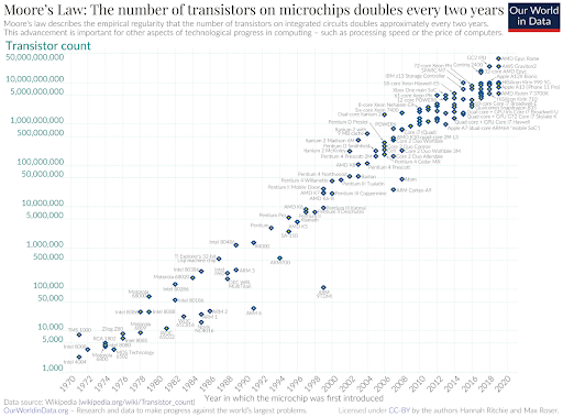
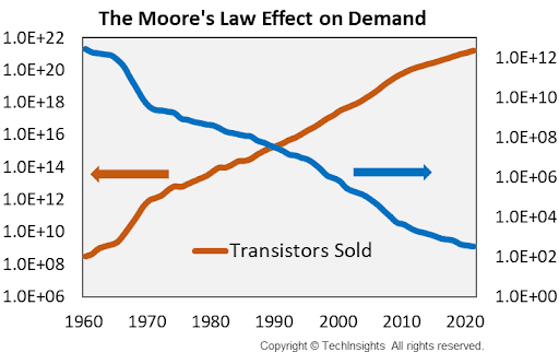
In the Age of Convergence, many forces are driving continuous advancement of semiconductor testing technology. As more and more functions are carried on a chip, and technology grows more and more complex, the number and types of test steps must be multiplied – leading, in turn, to increased test costs. Semiconductor test equipment requires ultra-long “standby,” which is an asset-heavy investment in semiconductor manufacturing plants, with a life cycle of at least 5 to 10 years. In an intelligent world where chip technology and processes are rapidly upgraded and iterated, such equipment must be able to meet increasingly complex testing needs at any time.

As a result, test and measurement solutions must expand to address the entire semiconductor industry value chain. This includes not only the traditional “center” of testing (IC production processes, wafer test and final test), but also greater integration with IC design and more system-level testing (SLT) at the product level, plus connectivity, including the cloud, artificial intelligence (AI) and Big Data.

Advantest and PDF Solutions’ collaboration [first announced in July 2020], targets these expanded capabilities. By combining PDF Solutions’ Exensio platform and its Data Exchange Network (DEX) with Advantest’s advanced test equipment (ATE), customers can connect and analyze data anywhere in the semiconductor supply chain, helping them improve product yield and reduce test costs.

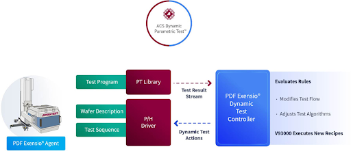
The two companies’ jointly developed product – ACS Dynamic Parametric Test (DPT) – integrates PDF Solutions’ Exensio data analysis products with Advantest’s V93000 parametric test system, enabling real-time optimization of parametric tests on the V93000 test platform and reducing manual interaction. The figure below illustrates the ACS DPT solution elements and functionality.

The balance of the article comprises an interview (also excerpted) with executives from both companies: Advantest’s Keith Schaub, vice president of strategy and technology, and Sonny Banwari, ACS vice president of business development; and PDF Solutions’ Guanyuan (Michael Yu), vice president of sales and operations, and David Park, vice president of marketing.

What are the key benefits of the Advantest-PDF collaboration, and why are they important for the semiconductor industry?

Keith:  Advantest has a long history in semiconductor testing, and we are the market leader in high volume manufacturing of semiconductor test products, with a range that spans from post-silicon validation, all the way to system-level test. Now, there is a lot of big data coming out of the test eco-system, and the industry has realized the future is using tools like AI and machine learning to mine data value, to improve the operational efficiency of the entire ecosystem, and of the entire supply chain.PDF Solutions is well established and strong in data analytics, and an ideal partner for bringing this advanced technology to the fore.

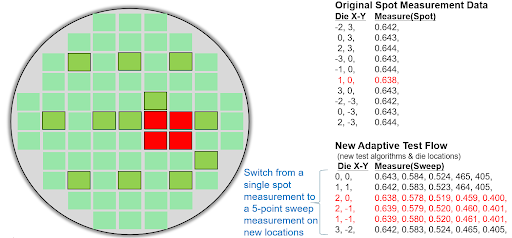
Michael: Advantest is the world’s leading supplier of semiconductor test equipment. Over the decades, it has amassed an enormous amount of knowledge and data related to semiconductor testing. PDF has always focused on data analysis of the entire semiconductor industry chain. The key point of this cooperation is to interconnect test-related data with the entire industry chain. For example, some data before testing, such as manufacturing-related data, can help to decide which devices to test and how to improve testing efficiency and quality. At the same time, data from these test cells can be brought forward to the subsequent steps of the supply chain and can also be fed back to obtain a more reliable and efficient test plan.

While the semiconductor industry is data-intensive, it is relatively backward in data analysis. What are the major obstacles? How will your joint data analytics-based products impact the industry?

Keith: The global semiconductor industry is in a period of rapid growth, and the huge market size brings huge growth opportunity for companies throughout the entire industry supply chain. At the same time, end-user applications are increasingly diverse and complex, with higher requirements for the quality and reliability of electronic components such as IC chips. Making test scheme coverage more comprehensive increases test cost. How do we control the cost of testing under the premise of ensuring higher quality? By mining the value of semiconductor data.

ACS powered by PDF Exensio is equivalent to providing the industry with an infrastructure platform for data analysis of the entire semiconductor supply chain. PDF Exensio can help collect data from semiconductor chip fabrication, test, and system-level test. With advanced algorithms, integrated workflows, and solutions delivered by ACS, more valuable information can be gained from the data generated by supply chain equipment and testing, resulting in shorter production times and higher overall equipment efficiency.

Sonny: As an example, the global chip shortage is a crisis for all industries, especially the automotive industry. In fact, this crisis has further forced carmakers to optimize products and technologies to deal with the chip shortage. The cooperation between Advantest and PDF Solutions is doing a similar thing: improving product yield through data analysis and providing customers with better products. It’s just reducing a company’s costs and improving its profitability, but it’s giving an opportunity for the entire semiconductor ecosystem to upgrade.

Michael: Indeed, to ensure the quality and reliability of chips, especially automotive chips, you need extensive testing, and that takes tremendous time and effort. But if we can adopt a traceable system and integrate the data of the entire production process, we can use AI and machine learning to tell us what to test, and what’s the most efficient way to perform the test. Instead of just one size fits all, with data analysis obtained through AI and machine learning, we can carry out personalized test plans for different quality requirements and find the best test results in the shortest time.

David: About five years ago, people were hesitant about going to cloud, mainly due to concerns about data security and privacy, especially in the semiconductor industry. This is the biggest obstacle for data analysis in the semiconductor industry. How to get enterprises across the supply chain willing to share data is a key step, and this is one aspect of what we are trying to do, to create a safe data sharing ecosystem. For example, both Advantest and PDF are involved in an initiative out of the GSA (Global Semiconductor Alliance) called TIES (Trusted IOT Ecosystem for Security), with the goal to bring together all the different players in the semiconductor supply chain, from design to manufacturing, packaging, and testing, to jointly form a secure trusted data sharing ecosystem.

Working remotely has also greatly promoted investments in cloud infrastructure, and the semiconductor industry is now a bit more open to moving data to the cloud. Being in the cloud will bring a more efficient and convenient data ecosystem to the entire semiconductor supply chain, for both scalability and computing performance.

In terms of empowering the semiconductor industry with intelligent means, such as big data analysis, cloud, and AI, what are the new trends in the future?

Keith: For a long time, the industry tended to use a one-size-fits-all general test solution, but different applications require customized test scenarios. However, with the increasing complexity of semiconductor process technology and the diversity of application requirements, the quality requirements for chips and other electronic components will also be different. Moreover, in the current environment of supply chain shortages, optimizing the test plan with different quality requirements for devices and use the big data analytics to control the test cost is vital. This is also what we are doing in cooperation with PDF Solutions.

Sonny: In the future, we will also increasingly tap the potential of AI-based and machine learning to develop more killer applications. Advantest and PDF understand each other, and we look forward to working together to elevate the power of machine learning to a new level in semiconductor testing and data analysis.

Michael:  As technology progresses, the manufacturing process becomes more and more complex; in addition, as chip size increases, there are more and more functions, which means that the amount of testing will also increase, and the whole process will generate an increased amount of data. And how to effectively leverage all of this data – through machine learning, AI, cloud computing and other methods, including data mining, to improve the overall efficiency of semiconductor manufacturing and optimize costs – will become more and more important.

Read More

Posted in Top Stories

Harnessing the Power of Data in Semiconductor Test

This article is a condensed version of an article published in the Winter 2021 issue of MEPTEC Report. Adapted with permission. Read the original article at https://issuu.com/mepcom/docs/meptec_report_winter_2021?fr=sNTRhZDE1OTk3NzE

By Ken Butler, Strategic Business Creation Manager, Advantest America

Every day, new methods are being developed to harvest, cleanse, integrate, and analyze data sources and extract from them useful, actionable intelligence to aid decision-making and other processes. This is true for a variety of industries, including semiconductor design, manufacturing, and test.

Moore’s Law (Figure 1) may be slowing with respect to traditional scaling of transistor critical dimensions. But as engineers continually develop ingenious ways to pack more functionality into a single product, e.g., 3D fabrication, multi-chip packaging, stacked die, and buried power rails (to name a few), the density of components in products is also increasing rapidly. Further driving this growth is an unprecedented increase in semiconductor demand, fueled by heightened online retailing, work-from-home scenarios, and transportation electrification.  

Figure 1. Illustration of Moore’s Law from 1970 to 2020.

One metric for tracking the overall semiconductor output is the number of transistors fabricated per year. VLSI Research [now part of TechInsights] has estimated that quantity for each decade since the inception of Moore’s Law, as shown in Figure 2, and estimates total output for 2021 was approximately 1.6×10²¹ (1.6 billion trillion) transistors!

Figure 2. Estimated number of transistors sold annually.

By even a highly conservative estimate, the test data resulting from this hard-to-imagine number of devices would be greater than 40 terabits per second! All that data must be analyzed – not only to determine which components are good and bad, but also for many other “bits” of intelligence: passing but “suspect” components, whether or not the product containing the components meets its datasheet and reliability requirements, whether or not the manufacturing and testing processes and equipment remain healthy and under control, and a host of other critical information.

Moreover, this estimate only addresses data generated by the test function and doesn’t include design, fab and test equipment, sensor, inspection, and calibration and maintenance data. So, we must deal with an ocean of data to streamline and optimize our production processes. It is a prime example of what Jack Morton from Bell Labs called the tyranny of numbers way back in 1958 [1].

Table 1 lists additional industry trends and associated test challenges that are changing today’s semiconductor test solution landscape.

Table 1. Industry trends and semiconductor test challenges.

Two facets of test significantly influenced by these trends are product quality and test cost.  New and subtle defect mechanisms, combined with the push toward ever higher levels of quality, increase the amount and complexity of testing and screening that must be performed to ensure low parts per billion test escape rates. All this testing, in turn, consumes more test time, thus increasing the cost of test. Semiconductor suppliers are looking largely to data analytics to solve these problems and keep the cost of test at reasonable levels without any compromise in outgoing quality or reliability. Let’s look at some examples of solutions Advantest is pursuing.

Dynamic parametric test

One of the earliest test steps performed on semiconductor devices is parametric test, also known as e-test or wafer acceptance test (WAT), which is performed during and following wafer manufacturing. The structures being tested can be individual transistors, resistors, and other components that are fabricated in the scribe lines, which are the small spaces between each die on a wafer, as illustrated in Figure 3 [2].  While these structures fill most of the scribe lines on the wafer, testing is typically limited to a few sites spread across the wafer surface.

Figure 3. Parametric testing involves structures fabricated in the wafer scribe lines between the die.

The test measurements provide valuable data used to monitor the health of the manufacturing process.  When anomalies are detected, typically the material flow is stopped so fab engineers can determine the cause of the problem. That often involves retesting material, collecting additional information, and performing additional manual analyses – all of which is disruptive and potentially costly to fab operations.

Dynamic parametric test (DPT) was created to automate and speed resolution of these types of excursions. Using DPT on an Advantest V93000/SMU8 parametric tester with PDF Solutions Exensio® software, a set of user-definable rules is established and checked during parametric testing. When the rules detect an issue, actions are immediately triggered to accelerate root-cause identification.

This process is illustrated in Figures 4 and 5. In this example, a diode measurement is being performed.  An out-of-specification measurement is detected, which triggers a DPT rule, and the test flow quickly adapts to a sweep of additional diode measurements across additional e-test sites on the wafer.  This real-time update collects the additional data necessary to diagnose the cause of the issue without requiring a stoppage of material flow and the reloading and retesting of aberrant wafers, thus saving both time and cost.  In the example cited here, the resulting root cause was quickly narrowed to a reticle or etch issue.

Figure 4. DPT detects out-of-spec diode parametric test.

Figure 5. DPT adaptively adjusts parametric test execution to collect additional data.

Production test edge computing

Downstream from parametric test is production testing. Wafer probe or wafer sort testing is performed while devices are still on the wafer. After good die have been singulated and packaged, they are subjected to final or package test. Other optional steps include system-level test, where die are subjected to a longer test that more closely resembles actual in-system operation, and burn-in, where the devices are tested, up to several hours, at elevated voltage and/or temperature to accelerate early life failures and measure product reliability.

Historically, production tests are a “one size fits all” proposition – for a given product, the same suite of tests is applied to every die. What’s desired, however, is to use data emerging from the test process itself to modify test content and execution so that each die sees the “right” tests. This process, which enables optimized deployment of test resources, is called adaptive test.

One form of adaptive test is executed as a post-test operation, e.g., wafer sort data is analyzed after the fact, and downstream final test operations are adjusted based on that analysis. However, semiconductor suppliers are also pursuing real-time adaptive test processes during production, in which test flow and content are altered during test execution, with low millisecond latencies. Several examples published in recent years describe scenarios that would work well when deployed as real-time adaptive test applications, including adaptive limit setting during search routines, predictive device trim, classifiers and device clustering, and burn-in optimization via at-risk device identification. [3] – [12]

Advantest developed ACS Edge to address this need for very fast, low-latency and highly secure analytics during production test. A high-performance compute platform with a dedicated, secure communication channel to the tester, ACS Edge wraps analytics in Docker containers to ensure reliable execution regardless of the compute environment’s configuration. All information related to the analytics and the data being analyzed is encrypted to prohibit unauthorized access that could compromise sensitive proprietary information.

Conclusion

As semiconductor product data sources become larger and more diverse, IC developers and manufacturers are challenged more than ever to deliver devices on time with highest quality and at the lowest possible cost. They are looking to advanced data analytics to extract intelligence needed to adjust manufacturing and test flows to adapt to an ever-changing environment. Test plays a pivotal role because it directly interfaces with each device to extract and analyze the data needed to monitor and control product quality and performance. DPT and test edge computing are just two approaches being deployed into production to address these challenges – we can expect to see more new solutions as innovation in manufacturing and test data analytics continues.


References

[1]  Various, “Tyranny of numbers,” 2021. [Online]. Available: https://en.wikipedia.org/wiki/Tyranny_of_numbers. [Accessed 22 Oct. 2021].
[2]  M. Bhushan and M. Ketchen, “Electrical Tests and Characterization in Manufacturing,” in CMOS Test and Evaluation, New York, NY, Springer, 2015. 
[3]  D. Neethirajan, X. C. K. Subramani, K. Schaub, I. Leventhal and Y. Makris, “Machine learning-based noise classification and decomposition in RF transceivers,” in IEEE VLSI Test Symposium, Monterey, CA, 2019. 
[4]  C. Xanthopoulos, D. Neethirajan, S. Boddikurapati, A. Nahar and Y. Makris, “Wafer-level adaptive Vmin calibration seed forecasting,” in Design, Automation and Test in Europe, Grenoble, France, 2019. 
[5]  M. Eiki, K. Schaub, I. Leventhal and B. Buras, “In test flow neural network inference on the V93000 SmarTest test cell controller,” in IEEE International Test Conference, Washington, DC, 2019. 
[6]  V. Niranjan, D. Neethirajan, C. Xanthopoulos, E. De La Rosa, C. Alleyne, S. Mier and Y. Makris, “Trim time reduction in analog/RF ICs based on inter-trim correlation,” in IEEE VLSI Test Symposium, Virtual, 2021. 
[7]  T. Y.-T. Kuo, W.-C. Lin, E. J.-W. Fang and S. S.-Y. Hsueh, “Minimum operating voltage preiction in production test using accumulative learning,” in IEEE International Test Conference, Virtual, 2021. 
[8]  M. Shintani, M. Inoue, T. Nakamura, M. Kajiyama and M. Eiki, “Wafer-level variation modeling for multi-site RF IC testing via hierarchical Gaussian process,” in IEEE International Test Conference, Virtual, 2021. 
[9]  M. Liu and K. Chakrabarty, “Adaptive methods for machine learning-based testing of integrated circuits and boards,” in IEEE International Test Conference, Virtual, 2021. 
[10]  S. Traynor, C. He, K. Klein and Y. Yu, “Adaptive high voltage stress methodology to enable automotive quality on finFET technologies,” in IEEE International Test Conference, Virtual, 2021. 
[11]  C. Nigh, G. Bhargava and R. Blanton, “AAA – Automated, on-ATE AI debug of scan chain failures,” in IEEE International Test Conference, Virtual, 2021. 
[12]  C. He, P. Grosch, O. Anilturk, J. Witowski, C. Ford, R. Kalyan, J. Robinson, D. Price, J. Rathert and B. Saville, “Defect-directed stress testing using I-PAT inline defect inspection results,” in IEEE International Test Conference, Virtual, 2021. 
Read More

Posted in Top Stories

Trends in Testing: New Challenges Create New Opportunities

By Doug Lefever, Senior Executive Officer, Advantest Corporation, and President and CEO, Advantest America

As advancements in semiconductors and microelectronics soldier ahead into emerging, even uncharted, territory, new test challenges arise. To that end, let’s look at a few key trends and challenges that are driving opportunities for innovation in the test sector.

Technology convergence has been a buzzword for some time, and this trend is only going to intensify with the heightened need to move, access, and analyze massive volumes of data. As a result, data analytics technologies (Big Data, artificial intelligence [AI], and machine learning) will continue to play a vital role in driving test efficiencies – not just operational, e.g., improving overall equipment efficiency (OEE), but also transformational: enabling data to feed forward and backward between test insertions, as well as outside of test. The reality is that the lines are blurring between the front and back ends of test, and the insertion points change, depending on device type and lifecycle status. So, the test flows that happen throughout the lifecycle of the device need to be flexible.

Complex high-performance computing (HPC) and AI devices are growing very large, and because of interposers and bridging, their power requirements can exceed 1000W. This means that we need to be able to manage temperature with a high degree of precision during testing. These large devices also require additional compute and analytics capability during test. To this end, we developed our ACS Edge solution, which essentially adds a supercomputer alongside the tester to open up compute power and start to enable real-time adaptive test.

With these developments, the system will become enormously complex, requiring verification of entire systems (hardware, firmware/embedded applications, and software). This means we’ll be seeing a broader deployment of system-level testing (SLT) for both systems and modules, as well as SLT/ATE at the probe level for known good die, including active thermal management solutions. To this end, we’ve incorporated into our offerings the test-related accessories we acquired upon purchasing Essai, including sockets, thermal control units and other test subassemblies. Our value proposition rests in our ability to address the full hardware stack and in the comprehensive nature of our offerings.  

In the broader test arena, generation, validation, and optimization of required test content such as scan vectors, built-in self-test (BIST), and functional test (software code) will need massive support and cooperation between the EDA and ATE industries. Advantest has established strong relationships with the leading EDA providers to help drive these efforts. The industry is also going back and mixing functional tests more with structural tests, and more design-for-test (DFT) techniques are being added. While increased scan, serial high-speed scan over USB, and PCIe ports are being used, that still isn’t enough, which brings us back to SLT continuing to be deployed.

For 5G, test solutions are largely in place. Some high-volume manufacturing (HVM) device interfacing/interconnect technologies like over-the-air (OTA) are coming along, while test development is starting for advanced millimeter-wave (i.e., THz, 6G). There will also more use of on-chip sensors and agents to monitor device performance all the way through the fab, assembly and in-field. This traceability is vital to ensuring ATE plays a critical role in pulling data from sensors – this heightened need for data extraction and analysis is a recurring theme that permeates everything going forward.

Continued electrification of cars will also drive lots of growth in test, including challenging areas like high voltages – i.e., those greater than 1kV – which require different kinds of methodologies. These higher voltage requirements are also needed for silicon carbide (SiC) applications in vehicles. SiC, like gallium nitride (GaN), has been around for a long time and is finding new life in applications such as battery management. We can cover this with our mixed-signal configurations and our integrated power solutions.

With respect to packaging, we expect to see a bifurcation in the industry: HPC/AI will move to 2.5/3D ICs, while mobile will remain on monolithic 2D for a little while longer. We’re already into 2.5 and 3D, and we have been for some time. However, with hybrid bonding and die stacking, we’re moving into 3D IC. When that is fully implemented, it will bring some tough new challenges. We believe a holistic approach is required to create high-power solutions that will then be coupled with other chips in a package.

In addition, there will be new approaches to address the “memory wall,” such as large eRAMs, 3D stacked RAMs, co-packaging on 2.5D or access via serial I/O. Power consumption of I/Os may also drive the integration of optical I/O. The first step will be co-packaged optics (CPO), which involves heterogeneous integration of optics and silicon on a single packaged substrate aimed at addressing next-generation bandwidth and power challenges. 

As you can see, many technology trends have test requirements that overlap or coincide, with demands created by massive amounts of data generation and processing playing a massive role. Testing at the exascale level requires powerful equipment that can handle the challenge. We are meeting this challenge with our EXA Scale test system, built on our flagship V93000 architecture, which addresses the challenges of very high scan-data volumes, extreme power requirements, fast yield-learning and high-multisite configurations.


Read More

Posted in Top Stories

Automotive Keyless Entry SoC Test Methodologies and Techniques

By Philip Brock, Applications Engineer & Consulting Manager, Louis Benton, Jr., Applications Engineer & Consulting Director, Advantest, and Jonvyn Wongso, Technical Staff Test Engineer, Microchip

Note: This article excerpts content from the Virtual VOICE 2021 Best Paper, voted on by conference attendees. Jonvyn Wongso, Daniel Marstein & Krishna Vangapalli from Microchip Technology co-authored the original paper, and their research and development efforts were invaluable to this project.

Passive Entry Passive Start (PEPS) technology has become standard in the automotive market for keyless operation. A secure wireless communication system, PEPS enables to lock and unlock the vehicle, start and stop the vehicle without physically using the key. Electronic functionality embedded in the key fob to interact with the vehicle (see Figure 1) includes passive start and stop, passive lock, remote keyless entry, immobilizer, key fob wake-up, and key fob localization. These functionalities are controlled by the primary modules embedded within the fob itself. The immobilizer provides access to start the vehicle when the key fob’s battery level is low by placing the fob at the start button and pressing it.

Figure 1: This diagram illustrates how components within the key fob correspond to functionality in the car itself.

The PEPS-to-vehicle ecosystem requires several key modules to function that includes a low-frequency (LF) transmitter, an immobilizer, a Radio Frequency (RF) transmitter (key fob) and transceiver (vehicle side), as well as a microcontroller (MCU). Each module in the key fob poses specific testing challenges and restrictions, necessitating a test plan and flow optimized for the testing of the key fob’s circuit, as shown in Figure 2. 

Figure 2: The key fob architecture depicts the main components within the key fob and a representation of how each component is tested on the Advantest V93000 test system.

The coverage percentages at the upper right in Figure 2 represent the overall test flow’s test time. Approximately two-thirds of the test coverage is dedicated to the LF structure (analog) and the MCU (digital), with another 19 percent focused on power management and parametric tests. The remaining 6 percent of the test coverage involves testing of the RF module with transmission functionality at sub 1 GHz band with no RF reception capability.

The combination of test requirements to accommodate all the different technologies housed within the PEPS key fob makes it an ideal device for demonstrating the versatility of the Advantest V93000 SoC test platform, including the AVI64 and PS1600 pin cards. A test solution is designed with comprehensive methodologies to test every module in the key fob. The balance of this article summarizes the key aspects of the test approach.

PEPS test methodology elements

Digital

Digital testing utilizes two standard methods to communicate to the IC:

  • Serial programming interface (SPI) – Standard communication protocol is used to test all non-MCU (non-digital) structures via direct access to the RAM. However, due to the slow communication speed compared to HVSP protocol, the programming time to the EEPROM is approximately 10ms per byte.
  • High-voltage serial programming (HVSP) – Used for FLASH and MCU core test with fast access to the EEPROM, this proprietary protocol is much faster than SPI, with a FLASH and EEPROM programming time of 3 to 4ms per page (each page is 16 bytes long).

One key digital test that has to be performed is to measure the time to program a page to the FLASH (16 bytes). The page program completion time varies between devices. The typical test method to measure and detect the end of the programming time is by implementing a match loop counter opcode in the pattern vector as the device asserts a state of a pin to high when the programming event has completed. However, the implementation of this method prohibits the use of the PS1600’s Time Measurement Unit (TMU) function on the same channel pin in parallel to measure the page program time accurately.

The test methodology developed involved the use of the Rapid Development Interface (RDI) API, a code structure that wraps Advantest’s standard application programming interfaces (APIs). The API is based on object-oriented programming that encapsulates firmware commands, enabling seamless execution of multiple commands. This creates a competitive advantage by dramatically streamlining the software development, and with the V93000’s multiport capability, it enables higher timing resolution that can be achieved on a specific pin or pin group. The use of the comparator functionality allows to strobe for a level change in the signal for a fixed amount of time.

Power Management

The Brownout detection circuit in the PEPS is a challenge to test to achieve optimized test time. In a typical test method, a voltage sweep is conducted from high to low to detect the brownout state threshold, followed by a voltage sweep from low to high to search for the recovery threshold level. An experiment was conducted with the implementation of four different test methodologies to determine the most optimized method to test the Brownout Detection circuit, summarized in Figure 3. In summary, the implementation of the Per Pin Parametric Measurement Unit (PPMU) as the Arbitrary Waveform Generator (AWG) yielded the fastest test time with minimal test instrument latency dependencies.

Figure 3: Investigation of four different brownout detection methodologies – PPMU as AWG methodology consumes a fraction of the test time in comparison with the other three options

Low Frequency Test

The Receiver Signal Strength Indicator (RSSI) circuit in the key fob indicates the proximity and location of the key fob with respect to the vehicle. The 3D LF pins are transponders with signal transmission and detection  at a frequency of 125 kHz with detection amplitude levels as low as 1.0 mV peak differential. The LF test requires a complex on-board circuitry in order to source AWG amplitude levels from 1 mV up to 8 V peak. Due to the real estate demand from the load board to implement these circuits with amplitude ranges, the extra-large size load board is used, extending out on both sides of the tester’s field. The RSSI value may only be read out after the completion of conversion of the LF signal level from a specific register in the device. In addition, there is a register that may be continuously read to check for status of the RSSI conversion.

Therefore, the proper test methodology for this test is to implement the Condition Go-No-Go (COGO) API from RDI to continuously check for the status of the conversion. This method corresponds to the device’s application. However, due to the inherent long latency to judge each event using COGO (described in Figure 3), a one-time fixed time delay was implemented prior to the readout of the RSSI conversion.

The other primary LF test involved the transponder, which is used for the immobilizer. The key fob that is placed at the start button of the vehicle will be energized by the vehicle’s coil that is located around the start button to enable communication between the key fob and the vehicle. This test requires both the AWG and Digitizer (DGT) instruments to source and capture the modulated waveform on the LF pins.

The communication between the key fob and the vehicle compromises of three stages as shown in Figure 4 – startup (energizes key fob), write mode (vehicle transmit authenticated message to key fob) and read mode (key fob responses with another authenticated message). The post processing of both the sourced and received waveform uses custom Digital Signal Processing (DSP) functions along with built-in V93000’s DSP APIs. 

Figure 4: Transponder communication between key fob and vehicle on LF pins on key fob.

RF Test

The Amplitude Shift Keying (ASK) modulation is used to transmit RF authenticated signal from the key fob to the vehicle. It is critical to test the duty cycle of the modulated signal that has a period of 12.5 us, toggled by an external pin when set in test mode. The device itself operates at a 2 us period. Therefore, multiport has to be implemented for the sequencer to drive two groups of ports at different periods. This test methodology also includes RF site interlacing technique, taking advantage of the V93000’s eight-site parallel test capability with 2 RF FE24 cards. Figure 5 illustrates the test criteria and methodology employed. Post-processing involves the capture of complex waveform, conversion of the waveform to rms in order to create the burst envelopes, performing moving average to filter out noise and searching for all falling and rising edges to calculate the duty cycle. 

Figure 5: The transmit ASK duty cycle test methodology is summarized here.

Software/hardware techniques

The LF testing requires sharing of the AWG and Digitizer instruments (MCE 4 source and 4 measure units) across 8 sites, thus increasing test time and reduces multisite efficiency. The implementation of SEMI_PARALLEL block in the test method enables execution of a single test cycle, hence maximizing multisite efficiency. Sequencers connected to AWG and DGT are placed in the SEMI_PARALLEL block as shown in Figure 6. Method 1 is the most common implementation. However, the setup pattern will be executed more than once on the same site. In contrary, method 2 is the least efficient but may be an option if the setup pattern may only be executed once to each site to avoid change of the state of the device.     

Figure 6: Shown here are the two most common SEMI_PARALLEL block test flow methods for shared resources.

Another test method technique implemented as part of the test solution includes the use of both RDI and MAPI APIs to resolve per site device failure on a specific mode or event as shown in Figure 8. RDI is used for the initial generation and execution of the pattern. MAPI APIs are subsequently used to re-execute the RDI generated pattern to specific failed sites. This method allows the recovery of the device(s) within the test method to save test time and not applying stimulus and retesting already passed sites.

Figure 7: The combination of RDI and MAPI usage enables device per site failures to be resolved.

On the hardware side, the use of relay driver circuit (SN74LS04DR followed by MDC3105LT1G) enables the drive of eight relays simultaneously such as G3VM-41QR10TR05 only by using a single utility pin. This technique enables the implementation of many circuit paths on the load board but omits the need of a PMUX card in the tester. Subsequently, the test load board design requires calibration of every signal path and circuit for each test site. There is an on-board EEPROM that stores the calibration offset and losses. Due to the limitation of memory space in the EEPROM, every calibration value is compressed using IEEE754 floating point standard. Depending on the accuracy requirement, this method enables greater than 50-percent compression rating of a decimal value. 

In summary, there are many challenges in both hardware and software development to create a test solution for optimized test time and efficiency, as summarized in Figure 8.

Figure 8: Summary and challenges of PEPS key fob test solution.

Since this device is targeted for automotive application, it has to be tested at cold, room and hot temperature ranges. Temperature variations affects the performance of the circuitry on the load board and has to be calibrated for each temperature range. The MCU core has to be tested at multiple different voltage level that requires synchronization of the pattern sequencer for each level change. In addition, testing the LF circuit requires extensive changes in the AWG’s amplitude level that requires additional setup and execution time that may increase test time and lower efficiency.

Read More

Posted in Top Stories

HSIO Loopback Turns Challenges into Opportunities for Test at 112 Gbps

By Dave Armstrong, Principal Test Strategist, Advantest, and Don Thompson, Senior Director of Engineering, R&D Altanova

For both PCIe and Ethernet (IEEE 802.3) signals are getting mighty small. With PCIe 5 reaching 32 Gbps (NRZ at 32 GBaud) and 802.3 reaching 112 Gbps (PAM4 at 56 GBaud), typical eye-mask limits are shrinking. Consequently, test requirements for high-speed I/O (HSIO) test are becoming daunting.

HSIO test involves measurement of Tx eye height and width, confirmation that a receiver can detect a low-level signal, and confirmation that continuous time linear equalization (CTLE) is effectively compensating for insertion loss. In addition, the test must verify bit error rate and confirm that a receiver can receive an off-frequency or out-of-phase signal. Yet another requirement is DC access for continuity and scan test.

Traditionally, HSIO loopback has been the preferred approach to HSIO test, with a simple wire or capacitor connecting a DUT’s Tx to Rx inputs. Loopback itself comes in various forms. The simplest form is internal loopback in which the device talks to itself and never exercises the transceiver circuitry; it can test internal logic only.

Another method is AC-coupled external loopback which does exercise the I/O circuitry, but like internal loopback, it does not perform Tx/Rx eye tests, and it does not test pre-emphasis and equalization. AC-coupled loopback is easy to lay out on a DUT board, but the signal level the Rx receives is too low loss / too hot, making the test too easy. Similarly, when connecting channel pairs for loopback tests, the Tx/Rx pairs share the same PLL/DLL, again making the test too easy. 

There are some workarounds that can be used on an AC-coupled external loopback. Long circuit-board trace lengths could help make AC-coupled test more realistic, while connecting the Tx of one signal pair bank to the Rx of another would mitigate the problems of a shared PLL/DLL. And the addition of bias tees loopback circuits would support DC and continuity (Figure 1).

Figure 1. AC-coupled external loopback test with bias tees for DC test.

However, these loopback tests do not provide sufficient visibility into the DUT that would aid in diagnosis, making them ineffective, particularly at speeds as high as 112 Gbps.

With the addition of some high-performance MultiLane instruments, one can improve on the simple loopback tests significantly. The Advantest V93000 platform supports two very different approaches for HSIO test: 16-Gbps test with the Advantest’s Pin Scale Serial Link (PSSL) card or 112-Gbps test with the MultiLane test-head resident instrumentation. 

The MultiLane approach supports a 112-Gbps PAM4 bit-error-rate tester (BERT). Based on a benchtop BERT, the AT4039E is configured as an eight-lane cassette that fits under a V93000’s DUT board, keeping signal paths short. In a similar fashion, the AT4025-50, which is the heart of the approach suggested in this paper, is a 50-GHz digital sampling oscilloscope (DSO), configured with eight channels per cassette, with 32 channels maximum per system. This complements the BERT and also fits underneath the V93000’s DUT board. The different types of instrumentation have their own advantages and disadvantages, each leaving some gaps in measurement coverage (Table 1).

Table 1. Instrument-based test capabilities for NRZ and PAM4 signaling.

A combination of instruments and a technique we call “BIST plus scope-sampled loopback” can fill the gaps while keeping instrumentation costs low and test times short. BIST plus scope-sampled loopback adds a splitter that provides a signal path to the DSO (Figure 2). 

In contrast to the PSSL or a BERT where test patterns originate and are received, the scope-sampled loopback technique makes use of the DUT’s BIST circuitry to generate a pseudo-random bit stream. The DSO can monitor this data stream while it is looped back to the DUT receiver in order to provide a comprehensive report on device performance during this real-world usage. Not only does this provide the user with valuable parametric data on the SerDes performance, it allows one to clearly differentiate between Tx and Rx problems. This approach also provides 6 dB of attenuation, more closely mimicking actual operation than does the standard AC-coupled loopback test, thereby overcoming the drawback of a test being too easy. Adding a programmable attenuator can provide an even more thorough test.

Figure 2. AC-coupled loopback test with a splitter providing access to a digital sampling oscilloscope.

The sampled-loopback technique does require some DUT-board real estate. One example of an AC-coupled loopback circuit with a splitter paired with an attenuator requires about 234 mm2 vs. 48 mm2 for an AC-coupled implementation with bias tees. The valuable data a DSO can capture using the technique can justify the additional DUT-board real-estate cost.

Sampled loopback also poses DUT-board layout challenges regarding trace losses and via impedances at 112-Gbps frequencies.  Tester signals connect on the bottom of the DUT board and make their way to a socket on the top.  This requires multiple vias and several inches of matched PCB traces to ensure that each lane sees the exact same interconnect length and attenuation (Figure 3).

Figure 3. DUT board showing insertion loss and impedance discontinuities.

The margin of error is small, requiring high-speed dielectrics (lossy dielectrics are sometimes used to stress the link) with trace widths typically between five and seven mils and prioritizing loopback circuit placement to keep trace lengths kept short. 

DUT boards are typically between 0.200 in. and 0.300 in., which pose signal-integrity challenges for vias.  Tuned-impedance vias are required to reduce insertion loss and must be a key focus for successful DUT-board designs at 112 Gbps. Finally, socket performance is also critical, and the socket cannot be an afterthought.

High-speed design requirements mandate effective SI simulation and optimization with all circuits modeled and included in the simulation well before the design is completed. 

Once fabricated, careful VNA measurements should be performed to confirm that design goals were met. Fortunately, a tightly integrated design-to-fab process can meet the requirements of DUT-board layout to support the BIST plus sampled loopback technique. High-frequency design validation closes the control loop on the design-to-fab process, providing proof of simulation accuracy, proof of board fabrication execution, and proof of final board performance. 

Initially, adding sampled loopback on all lanes supports the use of many DSO channels during characterization to speed data gathering. In production, you can make use of the characterization data to determine which lanes should continue to be monitored. Ultimately, for a mature product, the hope is that the DSO is no longer needed to monitor any channels.

Sampled loopback offers several advantages. For example, production software can support sampled loopback with the addition of scope code to check the DUT output.  In addition, the scope serves as a calibrated observer, a function not available with a device communicating with itself in a standard loopback test. PLL/DLL/VCO issues are some of the most common issues with SerDes interfaces and are best detected with the scope approach.  Finally, scope measurements are much faster than BERT measurements. 

Table 2 shows the scope sampled loopback technique closes the gaps in Table 1.

Table 2. Test and measurement gaps closed through the use of the BIST plus scope-sampled loopback technique.

Conclusion

In summary, early data and experience suggest that simple internal loopback, which tests only the ability of a part to talk to itself, is inadequate for testing many high speeds ICs. The addition of a calibrated external instrument such as the MultiLane DSO via sampled loopback provides the ability to identify problems that would otherwise be missed at 112 Gbps. 

Advantest can apply its years of experience in high-speed digital test to help you implement a BIST plus sampled-loopback strategy, and R&D Altanova can assist with the design of the very complex DUT boards supporting 112-Gbps data rates for the V93000 tester.

Reference

This article is based on the award-winning VOICE 2021 presentation “HSIO Loopback—The Challenges and Obstacles of Testing at 112 Gbps,” by Dave Armstrong, Advantest, and Don Thompson, R&D Altanova. 

Read More

Posted in Top Stories

Study Confirms 1.82-mm Coaxial-Interconnect Design Target for mmWave ATE

This article is a condensed version of an article published March 12, 2021, in Microwave Journal. Adapted with permission. Read the original article at https://www.microwavejournal.com/articles/35583-development-and-verification-of-a-185-mm-coaxial-interconnect-for-mmwave-ate.

By Jose Moreira, Senior Staff Engineer, SOC R&D, Advantest

The adoption of mmWave frequencies for applications such as 5G and WiGig creates new challenges for the ATE industry, including the need for a reliable blind-mate interconnection between the printed-circuit-board (PCB) test fixture and ATE measurement instrumentation. An ATE system requires multiple types of interconnects (Figure 1). Spring-pin interconnects predominate for power and digital. RF and mmWave signals require coaxial interconnects, due mainly to the isolation requirements, not just the frequency range. The ATE must also automatically mate to the PCB test fixture without any kind of manual interaction. 

Figure 1: This depiction of Advantest’s V93000 ATE system top-side shows the different interconnects for digital, power, RF, and mmWave.

A key requirement is interconnect reliability; for mmWave ATE applications, the interconnect must support 20,000 insertions while guaranteeing ATE system specifications. A reliability study demonstrates that a blind-mate 1.85-mm coaxial interconnect achieves this design target with a significant margin.

Figure 2 shows the bottom side of a mmWave ATE test fixture and the different mating interconnects. For the spring-pin-based interconnect, a plated via connects to the spring pin tip and to a PCB signal trace, which is then routed to the DUT. A coaxial mating connector handles RF and mmWave signals. A coaxial cable from the coaxial interconnect in the test fixture connects to another connector close to the DUT socket. Unlike a PCB signal trace, the coaxial cable provides layout flexibility and, more importantly, significantly lower loss, since even a thin coaxial cable is less lossy than the best PCB signal trace.1 

Figure 2: This view of the bottom-side of an Advantest V93000 ATE test fixture shows the mating connectors and signal routing.

1.85-mm interconnect design

Reference [2] describes the development of a 1.85-mm blind-mating interconnect design (Figure 3), which provides mode-free operation to 70 GHz with no interconnect failure for 20,000 docking cycles. The IEEE 287 standard-compliant3 1.85-mm female interface on the nonmating side of the interconnect uses off-the-shelf 1.85-mm cable assemblies to connect the blind-mating interface to the ATE measurement instrumentation and to the connector in the PCB test fixture close to the DUT. 

Figure 3: The blind-mating spring-loaded 1.85-mm interconnect requires mode-free operation to 70 GHz with a guaranteed 20,000 docking cycles.

Figure 4 shows the 1.85-mm blind mating connector pairs implemented on the ATE system and DUT test fixture sides. The system supports a maximum of 64 mmWave interconnects. The connector interface is spring-loaded on the male, ATE interface side and designed to self-align as the interface is mated. The mating action is part of the test fixture docking process to the ATE system. The ATE interconnect interface (Figure 2) comprises several interconnects apart from the 1.85-mm blind-mate connectors, all of which require a large docking force and, in turn, require special care with the mechanical design of the entire docking interface. This blind-mating interconnect requires a constant specific pressure on the entire mating surface to achieve the required 70-GHz frequency bandwidth. If this pressure is not correct or homogenous, effects like in-band resonances will appear in the interconnect frequency response.

Figure 4. This illustration depicts 1.85-mm blind mating connector pairs implemented on the ATE system and DUT test-fixture sides.

Reliability measurement procedure

Unfortunately, no clear guidelines have been published for evaluating the reliability of a blind-mate interconnection. Using the IEEE 287 standard3 as a guide and considering available resources, we developed a reliability test plan using a set of 14 connectors. Ten connectors were used for a docking cycle test to the maximum number of 60,000 insertion cycles. We measured S-parameters after every 300 cycles and removed the connectors to perform optical and mechanical measurements after every 6,000 cycles. Due to measurement resource limitations, we tested only two interconnects in parallel.

To eliminate the possibility that individuals in a pair become adapted to each other across the test run, after every 6,000 cycles, we exchanged the female of the pair between the two connectors being tested in parallel. Otherwise, measured reliability results could be significantly better than what you would find in a real application, where different test fixtures connect to different ATE systems through the lifetime of the connector.

Two other connectors were stressed to 60,000 cycles; in this case, only contact resistance measurements were performed every 300 cycles. Similarly, the same physical measurements and female connector exchange were performed every 6,000 cycles, as previously described.

Finally, the remaining two connectors in the measurement set were subjected to an accelerated life test, where they were left in a climatic chamber for 72 hours at 85°C and 85% humidity followed by the 60,000-docking-cycle test, with S-parameters measured every 300 cycles.

Measurement results

Our reliability testing strategy generated an enormous amount of data, which is summarized below and discussed in detail in Reference [4]. 

The S-parameter measurement setup consisted of an Anritsu MS4647B VNA and a 4-port extension MN4697B as well as Megaphase RF Orange 1.85-mm measurement cables. The VNA was used without calibration, so the loss shown includes both the coaxial cables’ and the VNA’s intrinsic loss. We employed this approach because our objective is to measure variations of interconnect performance over an increasing number of docking cycles, not the intrinsic connector performance. 

Figure 5 shows the interior of one connector pair before the test, at 30,000 cycles, and at 60,000 cycles, showing degradation of the socket side in the female of the pair. 

Figure 5: These successive images depict the interior of the connector pairs at different numbers of cycles.

Figure 6 shows the measured S-parameters after 60,000 insertion cycles. Since S-parameter measurements were performed every 300 cycles, the graph contains 200 overlaid plots. After cycle 54,000, a resonance appeared in the measured insertion loss around 20 GHz, revealing a failure of the interconnect, even though it continued working at higher mmWave frequencies. The cause for the failures was a crack in one of the socket fingers. This is the same mechanism seen with all failed connector pairs—not surprising since finite-element mechanical simulation shows this point has the highest mechanical stress during connector mating.4

Figure 6. After cycle 54,000, a resonance appears in the measured insertion loss at around 20 GHz.

Figure 7 shows the measured |S11| and |S21| parameters for a connector with no resonance failures during the entire 60,000-cycle test. This measurement was done with a fully calibrated VNA before the start of the test and after the entire 60,000 cycles. The results show even after 60,000 cycles, measured insertion and return loss are still acceptable.

Figure 7. This diagram shows the measured |S11| and |S21| for a connector with no resonance failures during the entire 60,000-cycle test.

Additional considerations

Although from a test and measurement perspective, electrical performance is the critical metric, the IEEE 287 standard defines several mechanical metrics, including the connector socket’s withdrawal and insertion forces.3 Another important metric is concentricity, the difference between the center of the inner and outer diameters of the socket and pin. In addition, computed tomography (CT) provides additional information regarding connector reliability. Figure 8 compares the surface of the original connector at cycle 0 to the connector’s surface at cycles 12,000 to 60,000 by visualizing the deviation in microns of the connector surface compared to cycle 0. Resolution is in the range of single-digit microns. 

Figure 8: CT scans performed on one of the interconnect female connectors at different stages of the cycle testing show successive deviations.

And finally, it is worth noting that the 1.85-mm connector standard offers many advantages for the blind-mate interface. For example, the long length of mechanical engagement of the adapter housing protects the center conductor while acting as an electromagnetic interference shield. A recent Microwave Journal article,5 on which this article is based, provides more information on the connector, mechanical metrics, concentricity, and CT scanning as well as additional details on our connector reliability test plan and on the mechanical finite-element simulations we used to confirm the specific failure mechanism we detected.

Conclusion

Our reliability study of a blind mate 1.85 mm coaxial interconnect for ATE mmWave applications shows that the target of 20,000 insertions was achieved with a significant margin, since all the connectors in the study failed above 40,000 cycles, excluding the connectors that had the accelerated life procedure performed. 

Acknowledgments

We thank Kosuke Miyao, Andy Richter, Marc Moessinger, and Matthias Feyerabend from Advantest; the Advantest failure-analysis lab in Gunma, Japan; and Eric Gebhard from Signal Microwave. We also thank Professor Sven Simon and Peter Gaenz from the Department of Parallel Systems at the Stuttgart University for the CT scan measurements.

References

  1. J. Moreira and H. Werkmann, Automated Testing of High-Speed Interfaces, Artech House, Second Edition, 2016.
  2. B. Rosas, J. Moreira, and D. Lam, “Development of a 1.85 mm Coaxial Blind Mating Interconnect for ATE Applications,” IEEE International Microwave Symposium, 2017.
  3. “IEEE Standard for Precision Coaxial Connectors (DC to 110 GHz),” IEEE 287-2007, September 2007.
  4. A. J. Rodrigues Mendes, Reliability Evaluation of a 1.85 mm Blind Mating Coaxial Interconnect for mmWave ATE Applications, Master of Science Thesis, Instituto Superior Técnico, University of Lisbon, 2020. fenix.tecnico.ulisboa.pt/downloadFile/845043405507284/Final_Thesis_Antonio_81353.pdf.
  5. Moreira, Jose, et al., “Development and Verification of a 1.85 mm Coaxial Interconnect for mmWave ATE,” Microwave Journal, March 12, 2021. https://www.microwavejournal.com/articles/35583-development-and-verification-of-a-185-mm-coaxial-interconnect-for-mmwave-ate

Captions

Figure 1: This depiction of Advantest’s V93000 ATE system top-side shows the different interconnects for digital, power, RF, and mmWave.

Figure 2: This view of the bottom-side of an Advantest V93000 ATE test fixture shows the mating connectors and signal routing.

Figure 3: The blind-mating spring-loaded 1.85-mm interconnect requires mode-free operation to 70 GHz with a guaranteed 20,000 docking cycles.

Figure 4. This illustration depicts 1.85-mm blind mating connector pairs implemented on the ATE system and DUT test-fixture sides.

Figure 5: These successive images depict the interior of the connector pairs at different numbers of cycles.

Figure 6. After cycle 54,000, a resonance appears in the measured insertion loss at around 20 GHz.

Figure 7. This diagram shows the measured |S11| and |S21| for a connector with no resonance failures during the entire 60,000-cycle test.

Figure 8: CT scans performed on one of the interconnect female connectors at different stages of the cycle testing show successive deviations.

Read More