
HSIO Loopback Turns Challenges into Opportunities for Test at 112 Gbps
By Dave Armstrong, Principal Test Strategist, Advantest, and Don Thompson, Senior Director of Engineering, R&D Altanova
For both PCIe and Ethernet (IEEE 802.3) signals are getting mighty small. With PCIe 5 reaching 32 Gbps (NRZ at 32 GBaud) and 802.3 reaching 112 Gbps (PAM4 at 56 GBaud), typical eye-mask limits are shrinking. Consequently, test requirements for high-speed I/O (HSIO) test are becoming daunting.
HSIO test involves measurement of Tx eye height and width, confirmation that a receiver can detect a low-level signal, and confirmation that continuous time linear equalization (CTLE) is effectively compensating for insertion loss. In addition, the test must verify bit error rate and confirm that a receiver can receive an off-frequency or out-of-phase signal. Yet another requirement is DC access for continuity and scan test.
Traditionally, HSIO loopback has been the preferred approach to HSIO test, with a simple wire or capacitor connecting a DUT’s Tx to Rx inputs. Loopback itself comes in various forms. The simplest form is internal loopback in which the device talks to itself and never exercises the transceiver circuitry; it can test internal logic only.
Another method is AC-coupled external loopback which does exercise the I/O circuitry, but like internal loopback, it does not perform Tx/Rx eye tests, and it does not test pre-emphasis and equalization. AC-coupled loopback is easy to lay out on a DUT board, but the signal level the Rx receives is too low loss / too hot, making the test too easy. Similarly, when connecting channel pairs for loopback tests, the Tx/Rx pairs share the same PLL/DLL, again making the test too easy.
There are some workarounds that can be used on an AC-coupled external loopback. Long circuit-board trace lengths could help make AC-coupled test more realistic, while connecting the Tx of one signal pair bank to the Rx of another would mitigate the problems of a shared PLL/DLL. And the addition of bias tees loopback circuits would support DC and continuity (Figure 1).
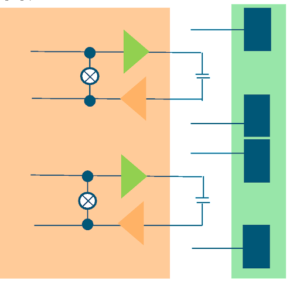
Figure 1. AC-coupled external loopback test with bias tees for DC test.
However, these loopback tests do not provide sufficient visibility into the DUT that would aid in diagnosis, making them ineffective, particularly at speeds as high as 112 Gbps.
With the addition of some high-performance MultiLane instruments, one can improve on the simple loopback tests significantly. The Advantest V93000 platform supports two very different approaches for HSIO test: 16-Gbps test with the Advantest’s Pin Scale Serial Link (PSSL) card or 112-Gbps test with the MultiLane test-head resident instrumentation.
The MultiLane approach supports a 112-Gbps PAM4 bit-error-rate tester (BERT). Based on a benchtop BERT, the AT4039E is configured as an eight-lane cassette that fits under a V93000’s DUT board, keeping signal paths short. In a similar fashion, the AT4025-50, which is the heart of the approach suggested in this paper, is a 50-GHz digital sampling oscilloscope (DSO), configured with eight channels per cassette, with 32 channels maximum per system. This complements the BERT and also fits underneath the V93000’s DUT board. The different types of instrumentation have their own advantages and disadvantages, each leaving some gaps in measurement coverage (Table 1).
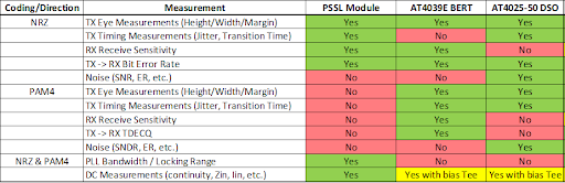
Table 1. Instrument-based test capabilities for NRZ and PAM4 signaling.
A combination of instruments and a technique we call “BIST plus scope-sampled loopback” can fill the gaps while keeping instrumentation costs low and test times short. BIST plus scope-sampled loopback adds a splitter that provides a signal path to the DSO (Figure 2).
In contrast to the PSSL or a BERT where test patterns originate and are received, the scope-sampled loopback technique makes use of the DUT’s BIST circuitry to generate a pseudo-random bit stream. The DSO can monitor this data stream while it is looped back to the DUT receiver in order to provide a comprehensive report on device performance during this real-world usage. Not only does this provide the user with valuable parametric data on the SerDes performance, it allows one to clearly differentiate between Tx and Rx problems. This approach also provides 6 dB of attenuation, more closely mimicking actual operation than does the standard AC-coupled loopback test, thereby overcoming the drawback of a test being too easy. Adding a programmable attenuator can provide an even more thorough test.
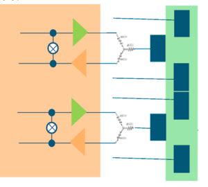
Figure 2. AC-coupled loopback test with a splitter providing access to a digital sampling oscilloscope.
The sampled-loopback technique does require some DUT-board real estate. One example of an AC-coupled loopback circuit with a splitter paired with an attenuator requires about 234 mm2 vs. 48 mm2 for an AC-coupled implementation with bias tees. The valuable data a DSO can capture using the technique can justify the additional DUT-board real-estate cost.
Sampled loopback also poses DUT-board layout challenges regarding trace losses and via impedances at 112-Gbps frequencies. Tester signals connect on the bottom of the DUT board and make their way to a socket on the top. This requires multiple vias and several inches of matched PCB traces to ensure that each lane sees the exact same interconnect length and attenuation (Figure 3).

Figure 3. DUT board showing insertion loss and impedance discontinuities.
The margin of error is small, requiring high-speed dielectrics (lossy dielectrics are sometimes used to stress the link) with trace widths typically between five and seven mils and prioritizing loopback circuit placement to keep trace lengths kept short.
DUT boards are typically between 0.200 in. and 0.300 in., which pose signal-integrity challenges for vias. Tuned-impedance vias are required to reduce insertion loss and must be a key focus for successful DUT-board designs at 112 Gbps. Finally, socket performance is also critical, and the socket cannot be an afterthought.
High-speed design requirements mandate effective SI simulation and optimization with all circuits modeled and included in the simulation well before the design is completed.
Once fabricated, careful VNA measurements should be performed to confirm that design goals were met. Fortunately, a tightly integrated design-to-fab process can meet the requirements of DUT-board layout to support the BIST plus sampled loopback technique. High-frequency design validation closes the control loop on the design-to-fab process, providing proof of simulation accuracy, proof of board fabrication execution, and proof of final board performance.
Initially, adding sampled loopback on all lanes supports the use of many DSO channels during characterization to speed data gathering. In production, you can make use of the characterization data to determine which lanes should continue to be monitored. Ultimately, for a mature product, the hope is that the DSO is no longer needed to monitor any channels.
Sampled loopback offers several advantages. For example, production software can support sampled loopback with the addition of scope code to check the DUT output. In addition, the scope serves as a calibrated observer, a function not available with a device communicating with itself in a standard loopback test. PLL/DLL/VCO issues are some of the most common issues with SerDes interfaces and are best detected with the scope approach. Finally, scope measurements are much faster than BERT measurements.
Table 2 shows the scope sampled loopback technique closes the gaps in Table 1.
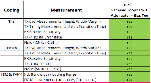
Table 2. Test and measurement gaps closed through the use of the BIST plus scope-sampled loopback technique.
Conclusion
In summary, early data and experience suggest that simple internal loopback, which tests only the ability of a part to talk to itself, is inadequate for testing many high speeds ICs. The addition of a calibrated external instrument such as the MultiLane DSO via sampled loopback provides the ability to identify problems that would otherwise be missed at 112 Gbps.
Advantest can apply its years of experience in high-speed digital test to help you implement a BIST plus sampled-loopback strategy, and R&D Altanova can assist with the design of the very complex DUT boards supporting 112-Gbps data rates for the V93000 tester.
Reference
This article is based on the award-winning VOICE 2021 presentation “HSIO Loopback—The Challenges and Obstacles of Testing at 112 Gbps,” by Dave Armstrong, Advantest, and Don Thompson, R&D Altanova.