By GO SEMI & Beyond Staff
At the start of the new fiscal year in April, Advantest Corporation officially appointed Doug Lefever as its new Group CEO. Lefever has been with the company for 25 years, serving as Corporate Vice President, Group COO, and President & CEO of Advantest America prior to his new role. We interviewed Lefever to learn more about his plans as CEO.
Q: Could you start by telling us a little bit about your history with Advantest?
A: Advantest has been a major part of my life—and it would not be an overstatement to say that the company has helped to shape who I am as a person. I joined Advantest in 1998—just three years after I graduated from college. Since then, I’ve had the pleasure of watching this company grow into a global leader in ATE manufacturing. I have served in many different capacities in my 25 years with Advantest and have touched most parts of the company in some shape or form, growing long-lasting relationships with key customers and maintaining an in-depth knowledge of our test solutions. I’ve also had the valuable opportunity to participate in key business decisions that have played a part in Advantest’s success, such as the acquisition of Verigy in 2011, which is directly responsible for Advantest’s #1 position in SoC testers.
Q: What are your plans for steering Advantest through current industry challenges?
A: Under the leadership of Yoshida-san, we have achieved strong performance in the past few years, greatly increasing our revenues and market capitalization and becoming the world’s number one ATE supplier. To continue this success, we must focus on listening to our customers so that we can meet customers’ needs by supplying them with high-quality, cost-effective test solutions where and when they need them. To this end, we must remain flexible so that we can adjust to market and societal demands.
As semiconductor devices continue to become more complex, our role in solving testing challenges grows. Our customers face challenges in advanced packaging and temperature control. We need to invest more in advanced R&D to further research in test cells and test flows. This will require close collaboration with customers and business partners as we work together to overcome challenges. Our greatest strength is our customers. Our ability to respond and adapt to their needs, especially for mission-critical applications, is the biggest factor in our success.
Q: What unique traits/characteristics do you believe you bring to the role of CEO?
A: I believe that change and growth come from within, and I think communicating directly with employees and getting to know people within the company is very important. For example, I often host “Coffee Talks” at the offices I visit. These are casual, free-form dialogues where I invite employees to ask questions, discuss market trends, and talk about recent innovations. I like to build trusting relationships with our employees and engaging with them directly allows me to learn more about their perspectives.
I also see my technical background and long tenure at Advantest as having great value in promoting Advantest’s innovation and building customer relationships based on trust. This powerful combination is important to our continued growth and advancement.
Q: You will be the first American CEO in the company’s history. How do you plan to navigate managing a Japanese company with an American background?
A: Advantest is a global company with over 96% of our sales coming from outside of Japan. As such, I aim to bring a global perspective to the role while preserving Advantest’s roots. Our company was founded in Japan, and its corporate culture is deeply rooted in Japanese customs. I don’t want to change Advantest to fit an outside perspective. I aim to do the opposite: I want to bring Advantest’s unique corporate identity outside of Japan and expand the company’s global reach. I believe this will become even more important to our success and longevity as the semiconductor industry continues to grow around the world.
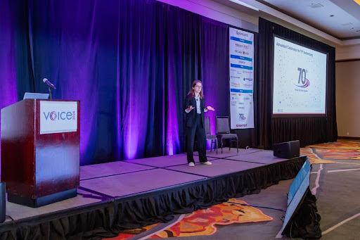
Q: Lastly, Advantest is celebrating its 70th anniversary this year. Could you say a few words about what this milestone means to you?
A: As I mentioned earlier, I have dedicated my entire career and most of my adult life to working for Advantest. This company is more than just a workplace for me; it is part of who I am. I am immensely proud to lead a company that has achieved such longevity and trust within the industry. We have been able to reach this milestone because we have not only kept up with but anticipated changing market needs. Moving forward, we will remain future-oriented and committed to achieving great things. We will also work wholeheartedly to fulfill our responsibilities to all stakeholders, including our planet. Achieving true sustainability in everything related to our company should be the cornerstone of our success.
I consider this milestone a huge achievement, and I am excited to commemorate it with my colleagues and industry partners in my new position as CEO.
Read More