Semiconductor Manufacturing and GlobalFoundries: How Essential Chips Drive Tech Innovations beyond 2024

Unlock the secrets behind GlobalFoundries’ ascent to semiconductor supremacy and find out how a colossal $1.5 billion boost from the U.S. CHIPS Act is setting the stage for technological innovation. Our guests, John Carulli, Ken Butler, and Shinji Hioki, join us from the frontlines of chip manufacturing to share their expertise on what it takes to be a pure-play foundry in today’s competitive market.
In this vibrant episode we track the transformation of silicon wafer dreams into the tangible powerhouse chips that energize our daily devices, dissecting the interplay of design, production, and the crucial customer relationships that drive the industry forward.
Feel the pulse of the semiconductor world as we tackle the elephant in the room: the pressures of Moore’s law and the herculean task of safeguarding tech’s most sensitive data. This episode is a call to arms for more transparent collaborations between foundries, assembly, and test operations, with an eye on the future where open data flow might just be the magic ingredient for enhanced yield management and efficiency.
As we wrap up our journey, we turn our attention to the fertile minds of tomorrow’s tech leaders. We discuss how acts like the CHIPS Act and mainstream conversations about semiconductors are sparking interest among the youth, encouraging them to pursue careers in this electrifying field. Our conversation weaves through the importance of engaging storytelling in tech education, making semiconductor testing and assembly as thrilling as time travel adventures for the next generation.
John Carulli holds seven U.S. patents. He has over 50 publications in the areas of reliability, test, and process development. He serves on the organizing or program committees of several conferences, including the International Test Conference, VLSI Test Symposium, and European Test Symposium.
Ken Butler is a Senior Director of Business Development in the Advantest Cloud Solutions (ACS) data analytics platform group at Advantest.
Shinji Hioki joined Advantest ACS in 2022, focusing on developing the ACS business in Japan.
Read More2024-2025 Semiconductor Industry Outlook with TechInsights (Podcast Season 2, Episode 12)

Prepare to be illuminated by the insights of Risto Puhakka from TechInsights as he joins us to map out the semiconductor industry’s explosive growth, driven by the thunderous influence of AI.
During our adventure through CES 2024, we bear witness to AI’s pervasive touch, from robotics and healthcare to the sizzling innovations in micro LED technology. Risto’s expert analysis doesn’t just skim the surface; it plunges into the economic, political, and competitive undercurrents that are redefining the semiconductor landscape.
Venture further into the conversation as we unravel AI’s sprawling web, extending its reach from agriculture to retail, and sculpting the semiconductor market’s future. We dissect the burgeoning world of spatial computing, and the surging demand for data streams, processor aptitude, and memory.
Gaze into the crystal ball with us as we reflect on 2023’s rollercoaster ride – spotlighting industry bottlenecks and breakthroughs – and cast our predictions for 2024’s market climate.
It’s not just a tech talk; it’s a strategic analysis of the global shifts, the CHIPS Act’s ripples, and how different nations are vying for supremacy in the AI arena. With Risto’s guidance, we’re decoding the blueprint of tomorrow’s semiconductor industry, where AI reigns supreme.
You can find this episode and more at this link: https://advantesttalkssemi.buzzsprout.com/1607350/14428141-2024-2025-semiconductor-industry-outlook-with-techinsights
Read MoreQ&A Interview with Leslie Tugman, SEMI
By GO SEMI & Beyond staff
As most of us in the electronics manufacturing supply chain are aware, the industry is facing a talent crisis and needs to fill the tech workforce pipeline with employees qualified to perform a plethora of available jobs. In this issue, we talk with Leslie Tugman, SEMI’s Vice President of Global Workforce Development and Diversity, about what SEMI and its member companies, which include Advantest, are doing to address this challenge.
Q. How are SEMI and its High Tech University (HTU) program driving industry workforce development efforts?
A. SEMI has made workforce development and talent advocacy a top priority and dedicated significant resources and expertise to tackle the talent shortage. We offer an extensive suite of programs and initiatives addressing the problem. All are available under our umbrella program called SEMI Works™, a holistic approach to workforce development that includes SEMI High Tech U, our University Connections and SEMI Mentoring programs, and SEMI Certs. These initiatives are anchored by an industry-wide competency model we are developing that will standardize and prioritize industry-acknowledged skills and support training programs linked to the skill sets the industry needs most.
Right now, the electronics manufacturing supply chain has thousands of jobs that it can’t fill. All of these jobs require skills across science, technology, engineering and/or math (STEM). This need intensifies as technology advances, and many K-12 public school systems around the world aren’t producing enough students with an interest or aptitude for high-tech jobs. The purpose of SEMI HTU is to inspire high-school students to pursue careers in our industry by showing them how these STEM skills are relevant and can be applied in the real world.
We take students out of their traditional classrooms and bring them to an industry site for a three-day intensive course. The company facility becomes their classroom, led by an instructor who works at that site and can tell students how they’ll use what they’re learning. The program combines lectures with hands-on learning and STEM exercises as well as lessons in communication, critical thinking, teamwork, and other career/life skills. The instructors serve as role models and provide a positive industry image.
Q. How do members participate in supporting SEMI’s workforce development programs?
A. There are a number of ways that members can participate in and support SEMI HTU. Members can sponsor HTU through financial and/or in-kind contributions. They can also participate by volunteering to teach a module at an HTU program. Participating in HTU is a great way for companies to support their corporate social responsibility (CSR) programs. SEMI can deliver the program for members, or we can train member companies to be certified partners to deliver the program independently. SEMI is currently delivering two HTU sessions per month around the world.
Q. How have HTU’s workforce development efforts evolved over the past five years?
A. The constriction in the semiconductor industry’s talent pipeline didn’t happen overnight; it’s been worsening for some time. In the last several years, a number of factors – including a greater shortage of talent, the shortage of STEM-educated students, biases related to gender and diversity, and the aging workforce – have converged to narrow the pipeline even more. At the same time, the number of job vacancies has skyrocketed. SEMI has become a leader in addressing workforce development in a broad, comprehensive manner. High Tech U, our mentor program and our diversity/inclusion initiatives focus on employee recruitment and retention.
We also have a University Connections Program that puts companies such as Advantest in contact with recent or imminent graduates so that they can help them understand why the company would be a great place to work. In the past five years, we have really embraced university students and young professionals as part of the audience we want to reach. SEMICON West will again feature a Workforce Development Pavilion that connects members with emerging talent through our HTU mentoring and University Connections programs. This is a significant area of focus at SEMICON West 2019. In addition, this year, we will conduct a High Tech U – which Advantest is co-sponsoring – in a classroom adjacent to the Workforce Development Pavilion.
It’s important to note that SEMI offers global workforce development initiatives. The need to fill thousands of industry jobs is global, although causes differ by region. For example, the aging workforce is a critical factor in Japan, lagging STEM skills are a key issue in the U.S., while shoring up the industry’s image in terms of diversity and inclusion is an issue worldwide. We tie this all together with a Workforce Development Council in each region that provides guidance and validation of our initiatives.
Q. Clearly, providing inclusive work environments will be vital to attracting new workers. How are you helping members rethink their corporate culture in this regard?
A. This is a critical component in terms of attracting future tech workers. Our CEO, Ajit Manocha, is passionate about diversity and inclusion. These kinds of efforts can fail when they don’t have executive support, and he is making this a top priority.
Mentoring is an important element in recruiting and retaining women in the workforce. Our new Spotlight on SEMI Women program honors women who are working at SEMI member companies and making a difference at every level. At SEMICON West, we will be celebrating our spotlight women at the welcome reception.
We also hold diversity forums on various topics – including unconscious bias and the importance of collecting data – to aid member companies in effecting internal change. Members like Advantest have been instrumental in supporting these efforts. In addition to its HTU sponsorship and partnering in workforce development, Advantest is active on both our Workforce Development Council and our Diversity and Inclusion Council.
Q. How can readers get involved?
A. There are a variety of ways to involve your company in SEMI educational activities. Here are a
- Attend a SEMI Diversity Forum: Next opportunity is April 18, 2019, at SEMI headquarters in Milpitas. Click here for more information and to register: https://www.semi.org/en/connect/events/semi-diversity-forum-2019-unconscious-bias-and-thought-diversity-tech
- Sponsor or volunteer at a SEMI High Tech U (Note: Advantest is sponsoring the HTU at SEMICON West, July 9-11, 2019, in San Francisco; for more information: judy.davies@advantest.com)
- Sign up to be a mentor or mentee through the SEMI Mentoring program. Contact: Csandoval@semi.org
- Attend a SEMI Diversity Forum: Next opportunity is April 18, 2019, at SEMI headquarters in Milpitas. Contact: Ltugman@semi.org
- Nominate a colleague for the Spotlight on SEMI Women recognition program. Go to: https://www.semifoundation.org/nomination-requirements-for-spotlight-on-semi-women/
- View and share the industry image campaign trailer: https://yourewelcome.org/en/
Q&A Interview with Ira Leventhal
 By GO SEMI & Beyond staff
This issue, we delve into a subject of growing interest in the test world and beyond: artificial intelligence. Our Q&A interviewee is Ira Leventhal, Vice President of Advantest America’s New Concept Product Initiative, a position he has held since June 2017. Ira has over 25 years of ATE industry experience, with Hewlett-Packard, Agilent Technologies, Verigy, and Advantest.
Q. Why is now the time for AI to be implemented in the semiconductor industry, given that it’s been discussed for many years?
A. Since Alan Turing first postulated in 1950 that the computer equivalent to a child’s brain could be developed and then trained to learn – evolving into an adult-like brain – we’ve been waiting for the technology to catch up to his theory. Today, all the key components essential to enabling AI are in place. First, you need a lot of data, and the Internet of Things facilitates this. Second, you need access to the data; using cloud computing and Big Data technologies, data silos become data lakes with easy access. Third, you need to fast data crunching, which we can achieve thanks to the tremendous advances in computational power and parallel processing. And finally, you need better algorithms for a wide variety of applications – the first three items have enabled rapid advancements in algorithm design.
Q. You state that advancements in deep learning will fuel the next semiconductor industry revolution. How so?
A. For years, the test industry has used adaptive test and other techniques to streamline and focus test efforts for maximum value (and minimum test times). With the advent of AI technologies such as neural networks, new possibilities are coming to light. Merging these approaches will allow the industry to improve device quality, reduce cost of test, and automate the control of functions best suited to the computers supporting us – freeing humans to concentrate on new developments and innovations.
Q. What is deep learning? Is it synonymous with AI?
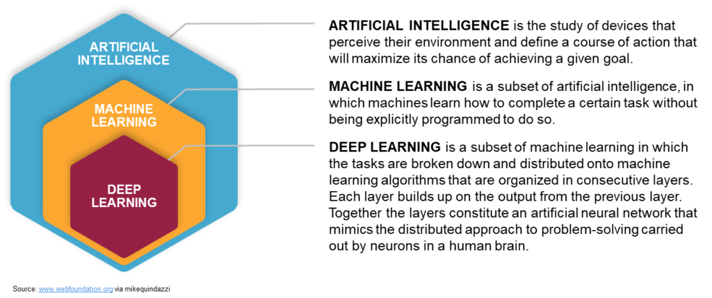
A. Many people don’t realize that AI, machine learning and deep learning are not interchangeable terms. AI is actually an umbrella term, and the others are nested subsets of AI. [See Figure 1].

Figure 1. AI vs. machine learning vs. deep learning
Q. Why should we focus on deep learning?
A. Deep learning is analogous to building a skyscraper. When you don’t have sufficient land to build a very large building, you go vertical. When you lack infinite storage, computing power and training data needed to build a very large single-layer neural network – which we do – you go deep. Deep learning promotes efficient use of available resources, much like a skyscraper, and it enables complex problems to be broken up into a series of steps, similar to an automobile assembly line.
Convolutional neural networks (CNNs) are used heavily in deep learning network architectures. When the network is being fed images during the training process, convolutional filtering layers are used that can recognize specific attributes of the images. As each layer views an image through a convolutional filter, it passes on a reduced set of data to the next layer, enabling the network complexity to be kept in control as you go from one layer to the next. The reduction in complexity of a CNN vs. fully connected networks minimizes processing, memory, and time required for image recognition. [See Figure 2.]

Figure 2. How a convolutional neural network works
Q. How can deep learning be applied in semiconductor testing?
A. A type of deep learning called transfer learning is well suited to our industry. Transfer learning enables you to start with an existing set of trained data instead of having to train a network from scratch. If you take a network that was trained with millions of images and you keep the initial layers that can understand low-level aspects of the images, you can replace later layers, training them on a new set of data for which you may only have a few hundred images. The result is a trained network that performs with significantly greater accuracy than if you’d started training from scratch. The reality is that a network trained from scratch would never catch up, no matter how long you trained it.
A key application is wafer metrology. Metrology involves monitoring your wafer process to make sure it’s staying within set limits by making measurements on the wafers over time. Trying to measure data on every wafer can be costly and cumbersome.
Virtual metrology (VM) is the prediction of wafer properties based on equipment settings and sensor data. This data is used with real metrology data from a sample set of wafers to create a deep learning model that maps process data to wafer metrology parameters such as layer thicknesses, photolithography critical dimensions, and others. Instead of measuring every wafer, you can measure a sample set, and then use VM to predict the metrology performance of the rest.
As geometries shrink and capacity is increased, new wafer processing equipment is constantly brought on line, and it is a big challenge to generate enough training data to keep the deep learning models current. Transfer learning enables you to build up a network that’s been trained on many different types of equipment. When a new piece of equipment is added to the line, you can tune a pre-trained network to operate with only a small set of data collected on that new piece.
Q. This is a fascinating subject. What other kinds of deep learning are there?
A. Reinforcement learning involves training a deep learning network on which actions will achieve the best ultimate reward. In this case, the network is like the brain of a mouse learning the fastest path through a maze to get to the cheese – it learns to navigate complex problems and come up with the optimal solution. An example is using deep reinforcement learning for production scheduling. Let’s say you’re trying to figure out how to minimize the overall time it takes to work through a complex multi-step production process from start to finish – the network will try different types of scenarios and figure out what works best.
Unsupervised deep learning has great potential for semiconductor manufacturing and test applications. Instead of telling the network what kind of data you’re giving it, you feed in unclassified data, and the network identifies things it sees that are similar to each other. It doesn’t know what those things are, just that they’re similar. It trains itself to classify things that look alike. This is powerful because you can throw a lot of unlabeled data at the network, and it will be able to identify relationships and act on them. It can find hidden relationships that humans might not have thought of, so unsupervised DL can do things that supervised DL can’t.
Advantest is working with university teams to investigate these techniques in detail, and we’re in discussions with multiple customers about ways to apply AI. We view it as a vital competitive advantage going forward.
Read More