The automotive semiconductor test market is experiencing organic growth as chipmakers produce higher volumes of devices serving an array of automotive applications. In addition, the range of applications for automotive-grade semiconductors is evolving as the technology advances. Manufacturers of automated test equipment (ATE) are adapting to ensure their systems can handle devices ranging from display drivers for all-electronic dashboards to silicon-carbide (SiC) power transistors for traction inverters.
Market data
The automotive industry’s use of semiconductors is growing, with carmakers now consuming about 8% to 10% of all semiconductors produced. This percentage is expected to rise as electric vehicles increase market share and as automakers outfit their vehicles with increasingly sophisticated advanced driver-assistance systems (ADASs). The trend is further driven by the increasing software content in vehicles to achieve higher levels of autonomy and by the migration of semiconductors once used primarily in luxury brands into mid-range and low-end cars over time.
According to Gartner, the worldwide automotive semiconductor market will grow from $67.5 billion in 2022 to $155.4 billion in 2032, when software-defined vehicles will surpass 90% of the total vehicles produced (up from 4.1% in 2022), unit production share of vehicles with internal combustion engines will drop below 60%, and autonomous vehicles above level 2 will reach 33.5 million, up from 4.2 million in 2022. (Level 2 implies partial driving automation in which an ADAS can handle steering and speed control, but a human must remain behind the wheel and be prepared to take control at any time.)
The automotive industry also presents demand fluctuations. At the height of the corona virus pandemic, for example, demand was aggressive and supplies were tight. Now, however, demand has moderated, supply chains have filled, and automakers have established second sources for many of the chips they require.
Expanding applications areas
Semiconductors have traditionally served a few primary applications in the automotive space. They have found use in engine control as well as the control of gear boxes, power windows, power steering, power brakes, seat heaters, and door locks. Microcontroller units (MCUs) typically handled the control functions, and they managed the sensors and actuators arranged in a distributed or zone architecture throughout the vehicle interconnected via a controller-area network (CAN) bus. For this scenario, a semiconductor test system that could test consumer-grade MCUs could easily handle the automotive MCUs, whose key difference was to meet automotive quality standards and to operate over the automotive temperature range. In addition, the standard battery voltage was 12 V, so most available power and analog tester resources would suffice.
Today, however, technology has evolved, and cars contain many different devices of heightened complexity and higher voltage ranges. The traditional functions such as engine and gearbox control remain, but their requirements have become more stringent as automakers pursue higher efficiencies and, for internal combustion engines, reduced emissions.
HPC moves into cars
In this new scenario, high-performance computing (HPC) typical of servers is moving into cars to implement increasingly sophisticated ADAS capabilities that perform safety/life-critical functions. To help implement the HPC functionality, automakers are moving from a distributed to a centralized architecture, which requires massive data transfer from sensors throughout the vehicle to a central electronic control unit (ECU) incorporating a high-performance microprocessor unit (MPU), which in turn necessitates high-speed automotive network interfaces. Automotive MPUs compared to consumer devices have to fulfill more strict quality aspects, so typically the test coverage is increased, outlier detection is applied, and a burn-in test flow gets introduced. In addition, testing across a wide temperature range from -40°C to +125/175°C is a must.
Voltages increase
Other factors resulting from the evolution of automotive electronics include the move from 12-V to 48-V architectures to power adjustable seats, windows, heaters, and even mild-hybrid traction motors. ATE makers are developing higher voltage and current instruments to test the devices that enable these higher voltage architectures.
Hybrid electric vehicles (HEVs) and fully electric vehicles (EVs) add further test considerations, requiring not just MCUs and other low-voltage components but battery-management-system (BMS) devices and high-voltage power modules as well. HEVs present some test challenges, but they operate at comparatively low voltages compared with EVs, and their battery-powered driving range is only about 40 miles.
In contrast, EVs delivering hundreds of horsepower incorporate converter electronics that can operate up to 800 V. In this respect, vehicle electronics is starting to resemble the electronics used in railway, wind-turbine, and solar-park applications, requiring high-power test methods. For EV traction inverters, automakers are increasingly turning to SiC devices because of their high-voltage capabilities and efficiency—SiC devices can extend the battery range of a high-end EV by an estimated 7% to 15%.
SiC technology can prove to be challenging. For example, operations such as regenerative braking can stress the SiC devices, and automakers need effective test equipment to ensure the devices work. Of particular importance is the short-circuit test, which requires fast turn-off of the device. The test system must protect the device under test, the handler, the probe card, and the tester itself throughout 100% device test.
Meeting traditional and new requirements
Semiconductor test companies must be able to cover the gamut of devices—including DRAM, flash memory, MCUs, display drivers, and power devices—for both traditional and new automotive applications. They can leverage their capabilities for commercial applications to automotive devices, where the key differences include temperature range.
Advantest offers a complete lineup of test solutions to handle all automotive semiconductor test applications. For traditional MCUs and similar components, the Advantest V93000 and T2000 platforms perform high-quality cost-effective test at high throughput. Both platforms feature a module-based architecture that enables flexible reconfiguration through the rearrangement of functional modules according to the application. Available modules offer digital, high-performance analog, and power-mixed-signal capabilities for testing a wide range of devices, including advanced automotive devices for ADAS applications.
In addition to requiring HPC MCUs, ADASs require inputs from cameras, radar, infrared, and other sensors, which versions of the T2000 and V93000 can accurately test. Other automotive devices requiring effective test solutions find use in applications ranging from airbag deployment and antilock braking, where test is vital due to safety aspects. The tests can be performed using mixed-signal versions of the T2000 or V93000. Similarly, RF configurations of those systems can test devices ranging from radar sensors to infotainment system components.
Vehicles will continue to incorporate a variety of other devices, including traditional MCUs for dashboard functions, with all-electronic dashboards also requiring display-driver integrated-circuit (DDIC) devices. Advantest’s T63xx Series testers address DDIC test requirements across the -40 to +175°C temperature range.
For devices that require higher voltages and power levels than standard car components, Advantest offers test capabilities up to 2,000 V or >150 A using ganged power VI setups. High accuracy is also an important parameter for testing the latest generation of BMS devices. BMSs perform battery charging, protection, cell balancing, and battery state-of-charge estimation. Battery management systems present significant test challenges as cell stacks present more cells per BMS chip and accurate voltage monitoring becomes increasingly important to maximize usable capacity and extend cell life.
To support BMS test, ATE will require high-voltage capabilities up to 160 V and the ability to provide highly accurate force and measurement performance <100 µV at high floating voltages. Advantest offers suitable and cost-effective test solutions to address all modern BMS ICs meeting the above requirements.
High-energy test
Test equipment for high-power devices such as those used in traction inverters requires even higher voltage, current, and power ratings. The market for high-energy (HE) test equipment used to be relatively small, focusing on railway, wind-turbine, and similar applications. However, the EV market is poised to expand the requirements for HE test equipment that can handle 400-V/800-V operation.
To address this market, Advantest in June 2022 acquired Italy-based CREA, whose products can test power devices manufactured by global semiconductor companies. The acquisition helps Advantest address the growing market for power semiconductors for a variety of efficient power devices, including SiC and gallium-nitride (GaN) implementations, as governments and industry pursue net-zero carbon emissions across a variety of applications areas—most notably the automotive industry.
The CREA product lineup features a chamber for bare die test that keeps temperatures under control and that maintains airflow to prevent sparking that can occur at high voltages. The company developed proprietary technology (called CREA LSI™) for its contacting system to achieve very low stray inductance, which improves device testability. CREA PCI technology provides protection for the device, probe card, tester, and handler against potential damage during short-circuit test, thus improving OEE (overall equipment efficiency) in production. In addition, the product lineup addresses the challenges of running high-energy tests in parallel.
The CREA product line complements the T2000 and V93000 to enable Advantest to provide full test coverage of the gamut of automotive semiconductor devices. Table 1 shows the full range of Advantest test solutions for semiconductor devices used across all automotive functions.
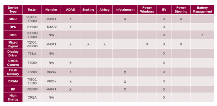
Table 1. Testers and handlers for devices and applications
Conclusion
As an automotive industry partner for many years, Advantest recognizes that electronics use in vehicles is evolving. Traditional electronic devices continue to find use, but new innovative products ranging from MCUs for HPC to power modules for use in traction inverters are becoming increasingly important. In addition, increasing electrification drives the need for more semiconductor testing to address high-demand, high-growth, complex requirements. Advantest recognizes the ever-broader requirement to create universal solutions that are customizable with user-friendly software to meet specific application needs. Advantest is uniquely positioned to see new technologies coming and to develop the solutions necessary to test them accurately, quickly, and cost-effectively.
Read More