Design Considerations for Ultra-High Current Power Delivery Networks
This article is adapted from a presentation at TestConX, March 5-8, 2023, Mesa, AZ.
By Quaid Joher Furniturewala, Global SI/PI Manager, R&D Altanova, Advantest
A power-delivery network (PDN), also called a power-distribution network, is a localized network that delivers power from voltage-regulator modules (VRMs) throughout a load board to the package’s chip pads or wafer’s die pads. The PDN includes the VRM itself, all bulk and localized capacitance, board vias, planes and traces, solder balls, and other interconnects up to the device under test. An optimized power-delivery approach will employ a decoupling scheme that provides low impedance to ensure a clean power supply. An optimized PDN will result in more power being transferred from the VRM to the DUT, with supply voltage held constant within a narrow tolerance band with minimal ripple under load.
PDN optimization is becoming increasingly important as more and more high-current applications appear. Keep in mind that power equals I2R, so even a slight amount of load-board resistance imposes significant power dissipation at high currents. For a 2.5-kW device, a 5% drop in power is 125 W! Table 1 shows how device voltage and current and load-board dissipation are trending over time.

Table 1. Device-power and load-board-dissipation trends
PDN optimization
For effective PDN optimization, prioritize the supplies, keeping in mind that not every supply can be optimized to achieve tight margins, and tradeoffs may be required. Also, plan your DUT board stacking based on power dissipation (Figure 1), and note that usually, the DUT vias account for the highest inductances in the PDN path. Plane inductance is negligible compared with via inductances.
As the industry moves to devices with high current demands, the historical rules of thumb and reference guidelines are no longer adequate. Following antiquated rules can lead to poor hardware design, requiring costly re-spins, dropped yields, and lost time. A proper PDN needs to be designed based on the device specifications to ensure a good power delivery network.
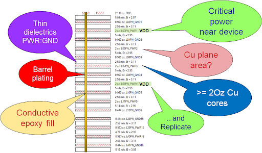
Figure 1. Plan your DUT board stacking to keep critical power near the device.
You can follow several recommendations when optimizing your load-board layout:
- Move or replicate critical power close to the DUT to reduce via impedance.
- Increase capacitor via size and use multiple vias at all capacitor pads.
- Put high-speed capacitors on the top side of the board.
- Use low equivalent series inductance (ESL) capacitors.
- Increase DUT via size to the extent permitted by your design-for-manufacturing (DFM) rules.
Contrary to popular belief, the under DUT capacitance (capacitor placed on the opposite side of the device on power vias) is not always effective. The capacitance may be dominated by the inductances of the long and thin DUT vias. Consideration needs to be given when choosing the value of the capacitance under the DUT. The least inductive way to effectively utilize decoupling would be to route the power closer to the device so that the DUT vias are short and place decoupling on the top side very close to the DUT with bigger vias.
When it comes to having the power delivered to the DUT with the least electrical resistance, offsetting the DUT vias towards the corner of the device to create a channel for current to flow to the device core can be a good strategy (Figure 2). If your DUT has high-speed pins or channels on a few quadrants, the others can still be offset to create a channel for the current to flow.
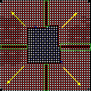
Figure 2. Offsetting the DUT vias toward the corner of the device can be a good strategy.
As the PDN return path on most ATE designs is shared with signal lines, the return path shares the return currents for the signal and power. Consequently, the return path becomes a non-trivial consideration. If the design has shared signal and power lines, the return path needs to be wide enough to ensure the current does not get constricted and create ground-bounce issues.
If the layer stacking allows for a GND-PWR-GND type structure, it is always recommended due to the noise coupling isolation and better power impedance. However, this is not practically possible in very dense and high site count designs where the thickness of the circuit board is limited due to the aspect ratio concerns with the fabrication of the board (aspect ratio is the ratio of the drill size to the board thickness). In this case, the GND-PWR-PWR-GND approach can be used (Table 2). It will offer slightly poor noise isolation but can be used for low-current and less noisy supplies, while GND-PWR-GND can be used for high-current supplies.
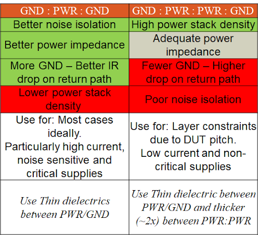
Table 2. Return-path considerations
PDN power-integrity (PI) analysis is a key to delivering ripple-free, low-noise, stable voltage to the device pads. PI analysis begins with a pre-layout analysis on all the power rails with the definition of your target impedance and decoupling strategy. Post-layout analysis is done after decoupling capacitance is placed and power is routed. Post-layout analysis includes all the PDN elements from VRM to DUT, and it involves DC, AC, and sometimes thermal analysis.
DC analysis
DC analysis examines via currents, current density, and voltage drop, including return-path voltage drop, due to resistances in the board current path. DC analysis helps identify bottlenecks due to copper depletion. Performance can generally be improved by increasing the copper area, replicating power planes, and increasing copper weights on stacks.
A case study involving a 2.4-kW device provides an example of DC analysis. The package includes a channel to provide better current flow near the core. The load board includes 2-oz copper layers with multiple high-current supply layers. A 1-mm pitch allows larger 14.5-mil power and return vias. Power shapes added in the signal layers based on available space help to improve performance. Table 3 shows IR drop simulation results for the various supplies. Total power dissipation is 83 W or less than 3.5% of the device’s 2.4-kW rating
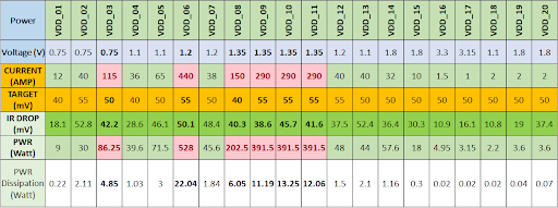
Table 3. DC analysis of load board for 2.4-kW device
AC analysis
AC analysis is the study to understand how the load ripples at varying frequencies. It is analyzed using impedance vs. frequency plots to determine whether the decoupling strategy is sufficient to meet the target impedance for the supplies.
At DC to the lower frequency ranges (<10 kHz), the region of lowest impedance on the ATE board is the ATE power supply region, and the path of least resistance is through the DUT power and return planes. As the frequency gets higher, the path of least resistance is through the bulk capacitors, high-frequency capacitors, and finally, the on chip capacitors, respectively. Capacitance on the PDN is designed to cover the entire device-clock-frequency spectrum in order to eliminate the voltage ripple generated by the device’s switching currents.
Each power rail requires a power-supply target impedance ZT as a function of voltage VDD, percent ripple, and transient current:

The target impedance calculations need to factor in the maximum ripple voltage that the DUT can tolerate (for example, 5% of VDD). It must also factor in maximum transient current, which is not always known. As a rule of thumb, ITransient is 50% of IMAX.
As an example, for a 10-A, 7.5-V VDD supply, a 5% ripple spec, and ITransient that is 50% of IMAX, the target impedance is 7.5 mΩ.
When determining target impedance, keep in mind that keeping impedance much lower than necessary will result in an overdesigned PDN and unnecessary cost.
Thermal analysis
Finally, thermal analysis involves studying temperature rise in circuit-board structures as currents increase. An effective strategy for thermal analysis is to employ PI-thermal co-simulation, which calculates heat generated as current flows through the metal structures of a load board from the VRM to the DUT.
Thermal analysis must consider the current flow from all supply rails but take into account the fact that not all supplies are necessarily activated at the same time. PI-thermal co-simulation is particularly useful for very high-power designs to identify hot spots that could cause damage to the board or DUT.
Thermal vias spread throughout the board with copper ground-flooding on the outer layers can minimize thermal problems. So can any additional structures, including frames and stiffeners, as they also act as heatsinks.
Figure 3 shows a thermal analysis that confirms satisfactory board temperatures resulting from supply currents. Supplies were run individually and in combinations of multiple supplies with a common return path. This simulation did not consider heat generated by components or the DUT itself.
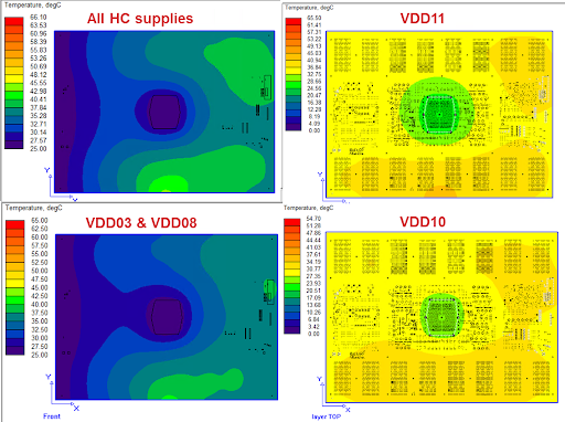
Figure 3. This thermal simulation shows heat generated by currents from individual supplies and combinations of supplies.
No matter how careful the design, thermal problems can appear during normal load-board operations. You can consider adding temperature sensors such as the Sensirion SHT35 and Texas Instruments TMP1075 to the board, placing multiple sensors on top and bottom sides in different locations. The sensors can communicate over an I2C interface and send an alert signal to the tester, which can be read on the tester pin-electronics channels when a temperature threshold is exceeded to perform a supply shutdown when needed.
Thin-core dielectrics and thick stacks
Other considerations in load-board design include the use of thin-core dielectrics and thicker stacks. Thin cores, such as 12-µm cores, are useful for printed-circuit-board power and ground structures. They permit higher layer density and lower plane inductances, offering impedance reductions of 10% to 45% compared to normal-thickness dielectrics (Figure 4). Note, however, that they are more costly, present handling risks, and may be hard to source.
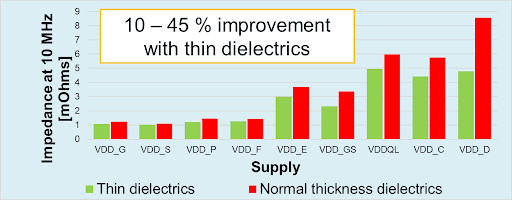
Figure 4. Thin dielectrics can provide a 10% to 45% improvement compared to normal-thickness dielectrics.
As for thicker stacks, existing ATE fabs offer board thicknesses up to 0.330 in. with a single lamination. Advanced fabs can create boards with thicknesses up to 0.400 in., increasing layer density by 21% (Figure 5). Thicker, higher-density stacks enable more layers for power planes. They are useful for CPU, GPU, and AI accelerator ATE boards, as well as memory probe and other probe tests. In addition, they support an increased number of layers with 2-oz copper cores to help improve PDN performance. R&D Altanova is in production of such boards effective this quarter.

Figure 5. Thicker, higher-density stacks can help improve PDN performance.
Conclusion
PDN performance is critical for the design of load boards for today’s high-current devices. Thermal concerns are increasingly significant as DUT power ratings increase. Design optimization and proper PDN power-integrity analysis will ensure that the power delivery is good without any power stability issues, thus increasing the yields for device under test. It will ensure a good working hardware and save precious time and cost for the board re-spins.
