
Die-Level Handling System Enables KGD Testing
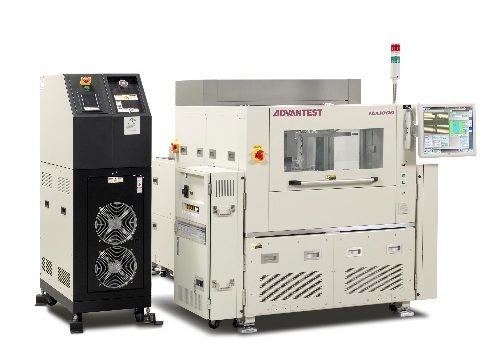
Advantest’s new HA1000 die-level handler is a cost-efficient test solution for determining known good dies (KGD) prior to IC packaging. It is the ideal solution for high-growth applications including mobile electronics and high-performance networking devices. With economics a driving factor in die-level testing, determining a semiconductor device’s viability prior to packaging or building memory stacks is critical to avoiding rework, achieving high yields and lowering costs. The HA1000’s ability to perform pre-assembly testing of singulated devices provides a new level of visibility into the quality of the device prior to committing additional devices and expensive packages to an assembly that could potentially have to be scrapped because of undetected problems.
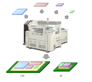
The new die-level handler allows full device testing to be performed before assembly, providing time-critical information that typically is only available at final test. HA1000 is designed to handle a wide variety of devices from large high-power server/GPU type devices to small systems-on-chip (SoCs) and memory devices/stacks, such as HBM2. The die-level handler can accommodate both thick and thin parts as well as stacks of 3D devices and partially or fully assembled 2.5D integrations. In addition, the HA1000 is ideal to probe fine-pitch pads, bumps, microbumps and pillars. Future applications of the system may also include probing of through-silicon vias (TSVs).
When joined together with the V93000 test system, Advantest provides a full test solution called the Die-Level Tester (DLT). This solution offers the following capabilities:
- Handles large, small, thick or thin devices.
- Can handle 3D stacks, 2.5D assemblies, and even partial assemblies.
- Vision alignment aligns the probes to pads, bumps, pillars or TSVs
- Automatic planarity adjustments to insure solid contact to non-flat surfaces.
- Integrated high-power active thermal control system to speed the testing of large complex designs.
- V93000 provides the ability to debug and test high-performance digital, analog, RF, and DC devices.
Target applications for the DLT reap a variety of benefits:
- Probing the singulated die just before assembly can improve final product yield while greatly reducing the cost of scrap.
- Active thermal control at the die level allows full final-test execution in order to maximize later yields.
- The DLT allows full testing of previously untested devices that may have been delivered from a multi-project wafer.
- The DLT performs KGD final testing of products to be delivered in die form.
- The DLT can speed time to market by allowing detailed device debug while blind product build takes place.
- The DLT can re-screen die-bank parts, allowing them to be re-programmed to meet new needs or tested to confirm performance to new requirements.
Most importantly, the handler’s precision vision alignment system precisely positions probe points to the finest pitch in use today. While properly positioning the chuck under the probes, the system can also adjust the planarity to match with the device surface to ensure a solid device connection. Its active thermal control (ATC) system enables the HA1000 to adjust on the fly to temperature fluctuations at the die’s surface over a very broad dynamic range of -40˚ C to 125˚ C. The temperature of the thermal head quickly responds using a hot-cold fluid mix. Thanks to low thermal resistance and high thermal capacity, the system can handle high-power devices with a thermal responsiveness often better than is possible in a packaged environment. This allows manufactures to test parts at higher power levels and/or tighter margins, which can improve yields while reducing scrap.