Pages Menu
Categories Menu

Posted in Featured Products

W2BI Unveils SmartBox – an Innovative System Level Test Solution for Smart Device Testing

By Artun Kutchuk, Vice President, Business Development & Strategy, and Keith Schaub, Vice President, Corporate Development, W2BI, Inc., Advantest Group Company

Combining W2BI’s patented QuikStressTM Automated Smart Device Test Software with 3D Robotics

Smartphones and other smart devices are continuously integrating new functions. Many of these functions are physical movements (i.e. NFC, vibration, gyro, compass, accelerometer, temperature, and health / fitness to name a few). However, most test solutions today still target the non-physical aspects — the software, applications, RF and other specifications. As a backdrop to facilitate our discussion, let’s focus on three key life cycle segments of the smartphone:

  • Pre-Launch production testing
  • Post-Launch / Reverse production testing
  • Point-of-Sale / In store diagnostics and testing

Each of these life cycles are closely related in the types of testing and diagnostics performed. To highlight that, let’s talk about some problems Alex, Tim, and Vicky are having with their smart devices.

Alex recently purchased a new smartphone but is having some audio issues when listening to music on his headphones. Tim has had his smartphone for about 6 months and recently his touchscreen hasn’t been working properly. Sometimes his phone doesn’t register when he swipes or presses the screen. Lastly, Vicky has been missing important phone calls and finally discovered when in silent mode, the phone isn’t vibrating like it is supposed to.

I’m sure many of you have experienced similar problems. Typically, the first thing you would do is to take your phone back to the Point-of-Sale (store where you purchased it) and inform the store assistant of the problem. Now what? Well, the assistant asks if you can show him the problem. Sometimes you can, when it’s a hard failure, but often you can’t. It might be intermittent, or occur only after certain events, or it might be caused by a specific combination of interactions between the hardware, software, applications, etc. Some stores have software diagnostic tools that perform a gross health check, but often the problem or issue is scenario based, therefore the diagnostic tool typically won’t capture or flag the failure, so the phone gets marked as NFF (No Fault Found), or NTF (No Trouble Found). Conservatively, we’ve estimated that NFF/NTF classifications are costing the industry in the 100s of millions of US dollars, perhaps in the billions.

There are two main reasons for that. First, in the store, the assistant typically will swap out your phone, giving you a new phone, so already a few hundred dollars to give the customer a brand new phone. Second, the NTF phone then churns through the reverse production line where numerous tests are run at multiple test stations looking for the problem, when no fault is found, the phone gets wiped and resold as a refurbished unit. Someone has to pay for all that testing and refurbishing. There are entire 2nd and 3rd tier markets existing largely based upon the high quantity of NTF/NFF phones. So, it would be safe to say that it is a big problem when the problem itself subsidizes entire markets.

There is a rule of thumb in industry for an end-user:

  • In the first occurrence of the problem –> Change the phone
  • In the second occurrence of the problem –> Change the Operator

The first time a customer has a problem with his phone, the customer is annoyed, would most probably change the phone – get a new one or upgrade to a newer model. If the store had to send his phone to the repair center, then he is without his phone for several days.

Then second time he has a problem, now he is extremely frustrated. The operator didn’t fix it the first time, and now he has to go through this again, so there’s a very good chance that he will switch operators.

You might ask. Didn’t any of this get tested at pre-launch? In fact, yes, smart devices with their myriad of integrated functions including: audio, touch screen, video, FM, BT, WiFi, NFC, compass, gyro, accelerometer, etc.), literally require a small army of people manually testing each function. The testing is highly subjective and prone with human errors and each function is generally tested standalone – that is, non-scenario based. Additionally, the emerging Internet of Things (IoT) devices are further complicating testing with high mix and low volume complex test setups.

This has created a need for a new platform that is low cost, easy to use, and automated consisting of robotics, and system level software able to interact and test functions, user scenarios, mission modes, and applications.

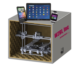
At W2BI, we developed an innovative platform, SmartBox, that:

  • Functionally tests key components of a smart device at pre-Launch Production, Point of Sale (POS) and Repair Depots completely automated with typical end-user scenarios
  • Scales the features and functions appropriately for the three key market segments (i.e. Pre-Launch, Point Of Sale, Post-Launch)

w2bi-img2The Key Values & Benefits to customers

  • Reduce NTF/NFF
  • Isolate quality issues
  • Classify true failures
  • Eliminate subjectivity
  • Verify & validate repairs
  • Increase Customer Satisfaction

W2BI’s SmartBox platform combines robotics with system level software designed to be a low-cost scalable profile with a simple and easy to use experience for Production Testing, Point of Sale and Return Depot end users. All major functions as well as integrated applications and user scenarios can be tested automatically.

w2biIn addition to testing the software, OS, UI, applications, and user scenarios, SmartBox will be able to test the physical functions, namely:

  • Touchscreen
  • Audio / Video
  • Camera / Lights
  • Vibration
  • Accelerometer
  • Physical Buttons
  • Compass
  • NFC / Wireless Charging
  • Gyro
  • Temperature
  • Health & Fitness

With SmartBox:

  • Point of Sale: A store assistant can potentially place the smartphone inside, chose one or more tests including scenarios and within a few minutes get back a non-subjective actionable assessment.
  • Pass/Fail result. Reverse Logistics / Repair Centers: Quickly and easily verify a failure as well as verify a successful repair and eliminate subjective errors caused by manual testing.
  • Pre-Launch Production: Automatically test and verify all of the physical functions eliminating manual labor and human error.

About the Authors:

Artun Kutchuk has over 25 years of experience in wireless, aerospace, robotics, business process automation and software development. He holds an M.Eng. Degree from McGill University. Artun also has co-founded a start-up and holds several patents in mobile device testing and diagnostics. Prior to W2BI-Advantest, Artun held multiple positions at Carrier IQ, Ericsson, Interfacing Technologies and CAE.

 Keith Schaub has worked in RF & Wireless Semiconductors for more than 20 years. Keith is the author of Production Testing of RF and System-On-a-Chip Devices for Wireless Communications. He holds five patents on various wireless devices and test systems, founded two start-ups, and is an avid writer and publisher on wireless topics.

Read More

Posted in Top Stories

Advantest’s VOICE 2016 Developer Conference Issues International Call for Papers

Advantest has issued an international call for papers on semiconductor test solutions, best practices and innovative technologies for its tenth annual VOICE Developer Conference. Based on the success of holding VOICE sessions in China and the U.S. this year, the 2016 conference will again be held on both sides of the Pacific Ocean — in San Diego, California on May 10-11 and in Hsinchu, Taiwan on May 18 — with the unifying theme of “10 Wonders of Technology” in recognition of the 10th anniversary of VOICE.

globeVOICE 2016 will offer attendees comprehensive learning and networking opportunities, including technical presentations, a partners’ exposition, social gatherings and the first-ever presentation track focused on new solutions in design technology and materials for loadboards and probe cards from various companies. In addition, the San Diego event will be the site of interactive discussion sessions for users of Advantest’s V93000 and T2000 system-on-a-chip (SoC) test platforms, memory testers, handlers, test cell solutions, product engineering and test technology.

International Attendance

Each year, the world’s semiconductor industry personnel from leading integrated device manufacturers (IDMs), foundries, fabless semiconductor companies and outsourced assembly and test (OSAT) providers come together at VOICE to share ideas and information as colleagues.

“VOICE has always been an engineering conference — created by test engineers for test engineers — for sharing useful, relevant solutions and best practices that can be applied directly to today’s most pressing test challenges,” said Mark Nagel, chairman of VOICE 2016 and Advantest staff applications engineer. “Now with the expansion of VOICE to include product engineering content, our 2016 conference is a can’t-miss event. As we mark VOICE’s tenth anniversary, we’ll be celebrating how this developer conference has evolved and grown with the IC test industry while also recognizing the people and innovations that have made VOICE so successful. I invite the world’s test community to join us in paradise — the beautiful Paradise Point Resort & Spa in San Diego — and/or at our second international location, in Hsinchu, Taiwan.”

Informative Technical Presentations

The VOICE 2016 call for papers focuses on seven technology tracks:

  • Hot Topics concerns new market drivers and future trends including security and encryption, emerging wireless standards, test challenges at next-generation technology nodes, the Internet of Things (IoT), automotive solutions and smart houses.
  • Device-Specific Testing covers techniques for testing MCUs, ASICs, PMICs, automotive radar, sensors, memory, baseband, cellular, multi-chip packages and more.
  • Hardware Design and Integration includes tester/handler integration, probe and package loadboard design challenges of new package technologies and fine-pitch devices, and more.
  • Improving Throughput addresses test-time reduction, increased multi-site efficiency, concurrent testing, data analysis, and more.
  • Reducing Time to Market encompasses DFT, pattern simulations/cyclization, automatic test program generation, system-level test, and more.
  • New Hardware/Software Test Solutions focuses on solutions utilizing the latest hardware or software features.
  • Test Methodologies involves techniques for testing DC, RF, mixed-signal or high-speed digital devices.

Test developers are invited to submit their abstracts for consideration at either the San Diego or Taiwan locations, or both, by going to https://voice.advantest.com/call-for-papers. All submissions must be received by November 20, 2015. Accepted presenters will be notified in January 2016. Audience members at the conference sessions in May 2016 will vote for the best papers, with winning presenters receiving prizes.

Attending VOICE 2016

VOICE 2016 registration will open in January. Industry members interested in attending the San Diego event can reserve hotel rooms now by calling 1-800-344-2626 and mentioning Advantest America or by visiting the hotel’s website. To arrange hotel rooms for the Taiwan event in Hsinchu, email mktgcomms@advantest.com.

For more information about the VOICE 2016 Developer Conference, including sponsorship opportunities, please visit https://voice.advantest.com/ or email mktgcomms@advantest.com.

Read More

Posted in Top Stories

Optimizing the True Cost of Test for SSDs

By Scott West, SSD Marketing Manager for Advantest America, and Mark Webb, Industry Consultant at MKW Ventures

With market analysts forecasting that production of solid-state drives (SSDs) will rise to more than 200 million units per year by 2017, device manufacturers need a reliable, high-volume, cost-efficient test solution to serve this rapidly growing market.

For SSD makers, focusing solely on the cost of test (COT) can be misleading. COT is calculated by dividing a piece of equipment’s purchase price by its throughput. While this is a valuable metric, it provides only a snapshot of one point in the lifetime of a tester.

Look at Total Cost of Ownership

To more accurately gauge the economic performance of a tester over time, SSD manufacturers should look at the total cost of ownership (TCO), which takes into consideration not just an item’s initial price, but also longer term considerations such as operating costs and maintenance. For instance, the expense of load boards and consumable materials, power usage, floor-space requirements and operator costs all factor into TCO.

Other considerations include intangibles such as service and support agreements, the length of cycle times and the turnaround time in procuring spare parts. Even an ATE supplier’s “staying power” can affect TCO. This is because semiconductor manufacturers need reliable equipment suppliers that are guaranteed to be around to help them quickly ramp up capacity when needed, to continually find innovative ways to drive down the cost of test and to develop new test technologies to address tomorrow’s market opportunities.

Maximize Your ROI

Because not all testers are created equal, throughput and productivity levels often vary for different systems. So meeting a chip maker’s throughput needs could require only three testers from one supplier, but four systems from another. For example, a PC-based tester might handle 25,000 to 30,000 I/Os per second when testing SSDs with standard second-generation PCIe interface protocols. However, a high-performance system such as Advantest’s MPT3000 platform, equipped with both address and data accelerators, can test eight SSDs simultaneously. This highly parallel testing translates to 260,000 I/Os per second, a throughput boost that dramatically improves TCO.

Another factor to consider is changing market conditions. While rudimentary PC-based testers may come with a lower initial price point, systems that are optimized for flexibility – with scalable architectures, the versatility to test a wide range of today’s device designs and the forward-looking ability to be reconfigured to meet future needs – will provide significantly better TCO in the long run.

As an example, let’s look at a SSD production facility using PC-based test equipment that is turning out a 50-50 mix of devices with PCIe interfaces and SAS interfaces. If market demand shifts and the company wants to adjust its production to 67 percent PCIe devices and 33 percent SAS products, it would need to purchase and ramp up more PC-based testers to handle the additional PCIe SSDs while idling some of its installed SAS-compatible testers.ssd2

Only by using reconfigurable test equipment could the company accommodate the new product mix without buying extra capital equipment, dedicating more floor space and bringing in additional operators. Advantest’s MPT3000 tester can be repurposed quickly and easily by downloading new firmware for SAS, SATA and PCIe protocols, making it the most flexible and extendible single-system test solution for SSDs.

A Future Enabled by Flexible Testing

The MPT3000’s flexibility makes it an especially appealing tool for out-sourced assembly and test (OSAT) foundries, which offer SSD makers the opportunity to avoid capital costs in testing their devices. The OSAT business model is based on testing a wide variety of devices in high volumes for multiple customers so these foundry operations need highly versatile test equipment with true multi-protocol support in a single system. While the OSAT model is well established in testing most semiconductor devices, this approach is a new undertaking for the SSD market. Still, the advent of SSD-focused test foundries has strong potential to shorten the time to market and drive down the cost of test for new SSD products.

Young, fast-growing semiconductor markets are characterized by quick shifts in market demand, which force device manufacturers to be agile enough to quickly re-balance their manufacturing levels for various products. This puts a premium on highly flexible test capabilities. For the high-volume, cost-sensitive SSD market, Advantest’s MPT3000 system provides the optimal solution.

ssd1

Read More

Posted in Top Stories

Getting from R&D to IoT with the EVA100

By Anthony Lum, Business Development Manager, Advantest America, Inc.

EVA Article Figure 1

Figure 1

The Internet of Things (IoT) is one the most ubiquitous technology-related topics these days. It’s become one of the tech buzzwords that transcend discussion in trade publications and blogs, showing up regularly in consumer and business publications as speculation swirls about when, where and to what extent IoT products are being deployed. Currently, the broadest applications for IoT solutions are automotive environments, from which myriad products can be launched and controlled, and household uses, including appliances, lighting and environment controls.

In the semiconductor world, analog integrated circuits (ICs) represent a key aspect of IoT. The need for analog ICs has increased in near direct proportion to the number of smart wireless devices on the market. With IoT device volumes expected to top these numbers, analog ICs will play an even more critically important role due to the higher performance, tighter accuracy and longer reliability that IoT devices require. In addition, analog ICs are essential to the rapid device characterization and fast delivery of customer samples the engineering community demands.

R&D engineers previously addressed these challenges by employing classic rack-and-stack or PXI benchtop instrumentation. These solutions were the best fit because of their broad technical reach. However, time-perishable deliverables proved extremely challenging because R&D engineers faced the additional task of developing system software to control and integrate the non-automated benchtop solutions. This undertaking requires strong coding skills and a more comprehensive knowledge of each of the benchtop instruments’ operation than the engineers typically possess. Manual measurement, on the other hand, is cumbersome and hampers rapid turnaround of deliverables.

EVA Article Figure 2

Figure 2

One solution that addresses this range of challenges is Advantest’s EVA100 measurement system, whose step-function integration is a significant improvement over classic benchtop instruments. The EVA100’s “all-in-one” concept integrates functions for a hose of instrumentation – power supplies, 4-quadrant DC signal measurement units, pattern generators, logic analyzers, arbitrary waveform generators, digitizers and oscilloscopes – into a single, modular unit. Each of these functions replaces standalone, focused instruments necessary to perform comprehensive evaluation and measurement of linear, automotive and industrial devices. Figure 2 shows how the EVA100 greatly simplifies analog IC device setup and replaces the need for six standalone, classic, benchtop instruments.

The “all-in-one” EVA100, also nicknamed the “shoe-box,” has a small footprint and is lightweight, portable and runs on standard 120V AC – all of which facilitates moving the unit from desktop to desktop, or into the lab as needed. The same hardware and setup can be preserved at any measurement station or node, assuring data acquisition consistency and correlation.

Rapid turnaround can be inhibited by development of complex software. Historically an underscoped task that tends to takes longer than expected to complete, software development is also complex and depends on users’ experience and comfort level. Software development is not needed with the EVA100, thanks to its newly developed, highly intuitive software GUI. With its drag-and-drop operation, the software interface enables engineers to quickly and easily create device-focused measurement set-ups. Automatic report functions dramatically improve deskwork efficiency, providing clear documentation and data ready for publishing in device data sheets.

The EVA100 combines Advantest’s unparalleled ATE and benchtop expertise to synergistically deliver a benchtop-measurement system that is fully modular and delivers benchtop-accuracy hardware along with intuitive GUI software delivering a complete turnkey solution. Priced competitively to benchtop instruments to ensure maximize ROI, the fully integrated EVA100 is often lower priced than an equivalent piecemeal rack or PXI instrument configuration. With software also included as part of the system’s package, the IoT-optimized EVA100 solves the two-pronged challenge of rapid device characterization and high performance quantitative data for a wide range of analog ICs.

About the Author

Anthony Lum joined Advantest America in 2006 and is currently ASD Business Development Manager. He amassed over 25 years of ATE experience specializing in RF and Analog SoC device testing through roles as a test engineer, applications engineer, and test and applications management at Texas Instruments and HP/Agilent. He received his BSEE at Arizona State University in 1986 and has authored over 20 IEEE and industry papers.

Read More