Pages Menu
Categories Menu

Posted in Featured Products

Advantest’s New Modules and Test Head Extend the T2000 Platform’s Performance in Evaluating Automotive SoC Devices

Advantest Corporation has expanded the range of its T2000 platform with the launch of two new modules and a test head designed specifically for high-volume testing of devices used in automotive applications.  The new equipment is designed to enhance test coverage, enable higher parallelism and reduce the cost of test for system-on-chip (SoC) devices used in automobiles, a market segment that is projected to have a 9.6 percent compound annual growth rate from 2019 to 2022.

Semiconductor content in automobiles is increasing rapidly as ICs are becoming integral in everything from powertrains and infotainment systems to ADAS (advanced driver-assistance systems) and on-board safety features.   To reach their market potential, automotive SoCs require high-performance, cost-efficient test solutions.

The new RND520 test head has 52 slots, providing the highest pin count available with Advantest’s direct-dock testing option. As a member of the HIFIX (high-fidelity tester access fixture) product line, the new test head supports massively parallel wafer-sort testing.  It covers an area 40 percent larger than its predecessor while using center-clamp technology to ensure stable contact during wafer sorting. In addition, the test head can operate over an extended temperature range up to 175° C.

The enhanced 2GDME digital module leverages 256 channels to test a wide range of SoC devices used in automotive electronics including MCUs, APUs, ASICs and FPGAs operating at speeds up to two gigabits per second (Gbps). It features a dedicated high-performance parametric measurement unit (HPMU) for every 32 I/O channels, giving the unit an expanded current capacity up to 60 milliamperes (mA) for every I/O channel. The module also supports high-voltage applications by enabling electrical stress testing and arbitrary waveform generator (AWG) and digitizer (DGT) functions valuable for characterization purposes.

The new 96-channel DPS192A device power supply facilitates highly parallel testing of automotive SoCs with high pin counts.  This versatile module has a voltage range of -2.0 volts to +9.0 volts and a current range up to 3 amperes. The unit’s capabilities include enhanced slew-rate control as well as a trace function to evaluate power integrity, an averaging function that improves sampling rates for measuring supply currents and a continuous sampling function that enables a new test methodology for IDD spectrum measurement.

The highly flexible T2000 test platform is ideally suited for evaluating SoC devices and other ICs fabricated with small-lot, high-mix manufacturing methods.  The system enables users to respond rapidly to shifting market needs with minimal capital investment while also helping to reduce development times for new designs.


DPS192A

RND520


Did you enjoy this article? Subscribe to GOSEMI AND BEYOND

Read More

Posted in Featured Products

Evaluating a spring probe card solution for 5G WLCSP

By Krzysztof Dabrowiecki, Feinmetall GmbH, Thomas Gneiting AdMOS Gmb], Jose Moreira Advantest

With the deployment of the wireless 5G standard and its support for mmWave frequencies that allow gigabits-per-second data rates on the consumer market, the semiconductor industry needs reliable and low-cost test solutions. The 5G standard allows mmWave range frequencies from 24GHz to 28GHz—to frequencies as high as 44GHz, and possibly even higher.  To achieve these frequencies requires reliable, highly efficient, cost-effective chip packaging technology. 

From that point of view, wafer-level chip-scale packaging (WLCSP) offers one of the most compact package footprints, providing a high level of functionality, and a frequency range with low resistance and inductance path. Despite having a good thermal performance with a finer pitch interconnection to the printed circuit board (PCB), WLCSP is resilient to extreme variations in stress, drop, and vibration. At the wafer test level, WLCSP technology requires a good and consistent contact resistance, a relatively high contact force with short probes, and above all, an effective online cleaning together with easy onsite repair [1]. With respect to those electromechanical wafer test requirements and with added value such as a frequency performance higher than 28GHz, or a high current capability, the spring pin probe card technology is always a favorite on the test floor on account of its cost and versatility and worthwhile to evaluate for high frequency 5G mmWave applications [2-4].

To define the best possible probe card structure, detailed electromagnetic simulations and analyses are required. RF engineers have several modeling approaches available for this type of simulation, such as a lumped element model (SPICE), distributed element model, or 3D electromagnetic (EM) models. For this study, it was decided to utilize CST Studio Suite 3D EM simulation software.  It allows us to build and analyze an exact and detailed 3D-model of the probe card. A probe card acts as an interconnector on the signal transmission path between the wafer chip and automated test equipment (ATE). Therefore, it is vital to keep in mind that, besides the probe card, there are other challenges with respect to ATE and the PCB side.

On the ATE side, mmWave frequencies already present significant implementation challenges, including the measurement instrumentation and interconnect to the ATE device under test (DUT) test fixture PCB.

Figure 1

Figure 1 shows a picture of the bottom of an ATE mmWave test fixture, where it is possible to observe the blind mating connectors to the ATE system and the coaxial cables. They are connected to coaxial connectors, very close to the socket. The use of coaxial cables in the test fixture is essential because a coaxial cable is significantly less lossy than any PCB signal trace. The PCB test fixture challenges, however, are not the main subject of this paper.

The system assembly and modeling (SAM) framework was used to investigate and optimize a signal path. It consists of multiple individual components, such as wafer bump, probe head, and PCB. These are described by relevant physical quantities such as field magnitudes or s-parameters.  This paper is trying to find an answer and explore three objectives: 1) the impact of different materials and probe head designs on the mmWave performance, 2) analysis of s-parameters and crosstalk, and 3) the probe head design optimization to improve them. Crosstalk is also an important parameter that is taken into account. The presented analysis results reveal the impact of different structure probe head elements on the s-parameter results.

Simulation model

Figure 2

Figure 2 shows an example of what mmWave RF peripheral ports (AN1, AN2) might look like on a 5G DUT. The diagonal bump pitch is 0.4mm, with a bump height of 100mm. The distance, in a row, between RF bumps is 0.566mm. Initially, a spring pin was chosen with uncompressed length L=3.7mm, at working mode L1=3.5mm.  The PCB thickness was 3.8mm and used a hybrid stack-up of the FR4 and Tachyon 100G for dielectric material. The matched trace lengths were designed at 38.8mm. Because of the symmetrical PCB traces layout, the simulation was performed for the critical traces only and one-quarter of the PCB. The RF 3D model analysis includes the wafer solder bump, probe head, and contact with the PCB, in which the traces are included up to the connector locations. 
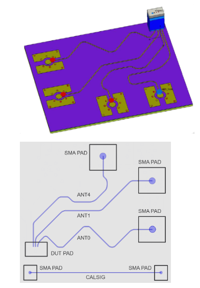
Figure 3

Figure 3 illustrates a quarter of the probe card model and trace topology.
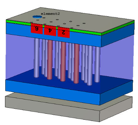
Figure 4

Figure 4 shows a model of a probe head in contact with the wafer at the bottom and the PCB at the top. The probe head is a 2-layer structure comprising guiding plates and fillers between the plates. The filler layers are the additional materials added between the guiding plates with various dielectric constants and loss tangent. The double plunger spring pins are inserted into drilled holes in the guiding plates and fillers. The pin plunger protrusions at the working mode are formed with a uniform air gap of 0.1mm between the head and the PCB, and 0.25mm between the head and wafer. The created 3D simulation model allows quick verification of results to identify appropriate material properties and geometry before building a test probe card.

Initial simulation results

It is well-known that any impedance mismatch in the signal path will have an impact on the return loss and in that way, degrade the measurement path performance. Therefore, impedance is a crucial parameter to be checked and controlled. In the PCB industry, the common impedance specification is in the range of 50 +/-10% Ohm for a single ended signal. But 5% is possible in certain cases, though at a very high cost.
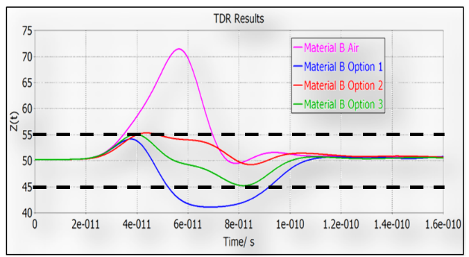
Figure 5

Figure 5 shows the simulated time domain reflectometry (TDR) plot for the model with various filler materials wit a time rise of 29.2ps (for 30GHz). The dashed lines indicate the maximum and minimum impedance tolerances. In the figure, it can be noticed that the air gap between the guiding plates causes an impedance discontinuity that peaks at

70 Ohms. The material option 1 shows a drop in the impedance discontinuity peak at 41 Ohm. The material B options 2 and 3 significantly reduce the impedance discontinuity to an acceptable range. As a consequence of material B air and option 1, the insertion loss and return loss had a limited frequency bandwidth, as shown in Figure 6. In this case, the dashed lines reveal acceptable limits of -1dB for insertion loss, and -10dB for return loss.

To read full article please visit Chip Scale Review December 2019 issue, page 14:  http://fbs.advantageinc.com/chipscale/nov-dec_2019/52/


Did you enjoy this article? Subscribe to GOSEMI AND BEYOND

Read More

Posted in Featured Products

New End-to-End Test Solutions for 5G, Automotive and IoT

Advantest’s new MPT3000ARC is the industry’s first test platform to combine thermal-control capability with high throughput, enabling extreme thermal testing of solid-state drives (SSDs).   Adding this new system to the MPT3000 product family, which is already in wide use by SSD manufacturers, Advantest is supporting SSD testing from design to manufacturing, providing the fastest, lowest risk path to market for next-generation devices, including PCIe Gen 4. In addition to meeting automotive thermal test standards, the new tester’s automation-ready thermal chamber enables SSD manufacturers to quickly ramp temperatures, which optimizes Reliability Demonstration Test (RDT) and results in faster time to market.  With the addition of the MPT3000ARC, the MPT3000 series enables rapid changeover to provide a single-system test solution for a wide variety of SSD products, from 40-mm M.2 memories to larger EDSFF devices.

The MPT3000ARC’s unmatched resourcefulness is a key advantage in the continually shifting and developing SSD market, designed to enable mission-critical testing across a broad range of SSD form factors and protocols. The single-system solution allows SSD manufacturers to easily evolve from testing PCIe Gen 3 devices to Gen 4 devices by simply changing a board and downloading firmware. This new tester provides the fastest path to bring PCIe Gen 4 SSDs to market while also minimizing risks, reducing test development time and accelerating new product validation, debugging and production tests.

The continuing growth projected for the solid-state drive (SSD) market requires device manufacturers to find a highly flexible test solution capable of supporting their expanding product portfolios at a low cost of test. Advantest’s new MPT3000ARC s tester is designed with the full spectrum of capabilities to handle all SSDs, including not only the most advanced PCIe Gen 4 memories, but also the highest performing enterprise drives and the most cost-effective client devices used throughout mass-market connected devices, from smart cars to wearable electronics.

With an increasing number of SSDs being used in rugged thermal environments, these memory devices must be proven to withstand harsh conditions. The MPT3000ARC features an innovative thermal chamber that allows it to operate over a broad range of temperatures, satisfying automotive and industrial thermal-testing standards. This makes the tester ideally suited for reliability demonstration testing (RDT) for the rapidly multiplying array of applications.

The MPT3000ARC applies the same proven architecture, software and performance already in wide use by SSD manufacturers worldwide. Its production-compatible ergonomics and automation-friendly chamber access make it suitable for high-volume SSD testing.

By using changeable and customizable interface boards, this tester has the versatility to handle virtually all SSD form factors, from 40-mm M.2 memories to larger EDSFF devices. The system’s design enables quick and easy switching of interface boards, enabling rapid changeover to support a wide variety of SSD products on a single system.

As the newest member of Advantest’s MPT3000 product family, the MPT3000ARC is fully integrated. Its efficiency and performance are optimized by leveraging the same tester-per-DUT architecture, site modules, power supplies and hardware acceleration as all other systems in the MPT3000 series.

View video to learn more.


Did you enjoy this article? Subscribe to GOSEMI AND BEYOND

Read More

Posted in Featured Products

New T2000 Module Has Industry’s Highest Analog Digitizer for Cost-Efficient Testing of High-Res Audio ICs

Advantest’s new GPWGD high-resolution module features the industry’s highest analog-performance digitizer, which supports testing of high-resolution audio digital-to-analog converters (DACs) embedded in power-management ICs (PMICs) as well as stand-alone high-resolution audio devices. The module’s innovative measurement technique performs over an ultra-high dynamic range, achieving unprecedented accuracy in analog testing from device characterization to mass production without requiring complex performance boards or additional test and measurement instruments on the T2000 test platform.

High-resolution audio features both a wider dynamic range and an improved sound source compared to CDs. The proliferation of electronic devices capable of supporting high-resolution audio – including smart phones, wireless audio components for wearable electronics and home theaters, automotive navigation systems, gaming consoles, 4K and 8K televisions, and other next-generation products – has led to an increase in the number of PMICs with embedded digital-to-analog converters (DACs), which require high-dynamic-range testing with 24-bit or 32-bit resolution.

When used on the T2000 platform, the GPWGD high-resolution module provides the versatility to test both PMICs and high-resolution audio DACs using the same system configuration.  This helps users to save on their capital investments while also reducing test cycle times.

The module’s upward compatibility and the high-resolution functionality of its digitizer enable industry-leading measurements with both a signal-to-noise ratio (SNR) and a dynamic range (DR) of 130 dB, surpassing the analog performance of other testers typically used by developers of audio ICs. In addition, the unit’s massive parallel site testing capability leverages twice the number of sites compared to other systems on the market, resulting in higher throughput and a lower cost of test.

The new GPWGD high-resolution module’s extendible design allows it to be seamlessly integrated into either laboratory or production environments for existing device types as well as new high-resolution audio ICs.

Read More

Posted in Featured Products

New V93000 Wave Scale Millimeter Solution Cost-Effectively Tests 5G-NR mmWave Devices up to 70 GHz

Advantest Corporation has extended its V93000 system to cost-efficiently test the next generation of 5G-NR radio frequency devices and modules on a single scalable platform.  The new V93000 Wave Scale Millimeter solution has the high multi-site parallelism and versatility needed for multi-band millimeter-wave (mmWave) frequencies.  The operational range from 24 GHz to 44 GHz and 57 GHz to 70 GHz enables customers to reduce their time to market for new designs running at mmWave frequencies.

The highly integrated system is architecturally distinctive from other solutions by providing as many as 64 bi-directional mmWave ports based on a modular implementation.  This allows not only the use of different 5G and WiGig frequency modules, but also the addition of new modules as new frequency bands are rolled out worldwide.  Based on an innovative mmWave card cage with up to eight mmWave instruments, this highly versatile and cost-effective ATE solution performs on the level of high-end bench instruments.  The scalable system’s wideband testing functionality gives it the capability to handle full-rate modulation and de-modulation for ultra-wideband (UWB), 5G-NR mmWave up to 1 GHz, WiGig (802.11ad/ay) up to 2 GHz and antenna-in-package (AiP) devices in addition to beamforming and over-the-air testing.

In delivering the industry’s first integrated, multi-site mmWave ATE test solution, Advantest is providing a pathway for customers to lower the cost of test for their current and upcoming 5G-NR devices while leveraging their existing investments in our well-established Wave Scale RF testers.  In particular, OSAT companies can benefit greatly from this flexible, scalable mmWave ATE solution.

Early installations at customers testing both 5G and WiGig multi-band devices have been completed.  Advantest is now accepting orders for the new mmWave solution.

Read More

Posted in Featured Products

High-Volume Consumer Devices Need High-Voltage Test Solution

by Anthony Lum, Business Development Manager, Advantest Corp.

If you’ve been increasingly feeling that your home doesn’t have enough electrical outlets for all of the consumer products you’re amassing, you’re not alone. As our hunger for consumer devices grows, so does our need for more AC-power wall outlets. The common denominator between large entertainment hubs, wearable and portable devices, and smart-home hubs/accessories is the need for AC power – either as a constant source or for on-demand recharging. Hand-in-hand with this requirement comes the need for reliable testing to protect these devices by ensuring their power supplies can handle the associated high voltage.

Most devices that plug into AC outlets need a power testing solution that can accommodate voltage as high as 2,000 volts (or 2 kilovolts). This is vital worldwide: both in industrialized countries, where the power supply is stable and reliable; and in developing nations, where little to no regulation exists on the power-supply side. In these regions, power surges and glitches that can damage or destroy an end product are not uncommon. As these devices are manufactured in high volumes, the more you have, the more important it is to preclude surging and overheating.

Enabling high-voltage testing

Previously, there have been two options for those seeking a high-voltage semiconductor test solution. Testing at-voltage, while the most accurate approach, incurred a premium cost for the device on the part of the chip manufacturer because it required building special, costly test equipment or using antiquated test systems as the high voltage source, but traded off quality of other functions and tests. Less costly: guaranteed-by-design ICs that weren’t tested in production because the chip provider deemed the added test costs not worth the investment internally. This requires trusting that the design will work in all circumstances without real-world testing to back it up. Monolithic ICs may contain multiple discrete power devices in a single package, further increasing the need for accurate, preventive testing.

Advantest has developed a cost-effective solution that achieves real-time testing in situations where testing wasn’t previously performed. A new module for its EVA100 measurement system allows testing of these high-power ICs deployed for large-volume consumer applications. This includes the power FET at the heart of all AC/DC and DC/DC converters.

The HVI (high-voltage VI [voltage-current] source and measurement module) ensures the reliability of power devices used in applications such as AC/DC or DC/DC converters (behind which are power field-effect transistors, or FETs) and LED drivers, as well as motor controllers, gate drivers and intelligent power modules (IPMs). It does this by accurately measuring their current leakage and breakdown voltages, utilizing unique capabilities designed into the module.

The HVI possesses a digital loopback architecture, which allows glitch-free changing of current or voltage mode, or range switching, on the fly. This is important because the test range isn’t a straight path from 0 to 1,000 (or 2,000) volts; there is an intermediate range that must be accommodated. The HVI module handles measurement across the entire voltage range with no spikes, yielding faster test times and more accurate results.

The HVI module excels at testing the breakdown voltage of power devices that go into AC/DC converters, i.e., the amount of voltage the device can sustain before it short circuits. Since manufacturers typically guarantee their products up to 800 volts, the module allows immediate ramp-up to 800-850 volts in order to ensure the device can sustain the breakdown voltage without failing (see Figure 1). Monitoring over time is key, as this allows the module to recognize variations in time and current as voltage increases, thus achieving more accurate test results.

Figure 1: This plot, in which two 800V ramps are overlaid on top of each other, provides an example of glitch-free voltage source measurement performed by the EVA 100 HVI module.

When using a single channel, the HVI module expands the EVA100 voltage coverage up to 1,000 volts with a current range of +8 milliamps or +20 milliamps of pulsed power.  By stacking the voltage source, the module enables tester coverage as high as 2,000 volts.  This ganging also enables the EVA100 to handle devices with a current range of +16 milliamps up to +40 milliamps of pulsed power.

In addition, the HVI module features digitizers on both the voltage and current source lines. This construct allows the EVA 100 to sample and monitor both current and voltage simultaneously, in real time, to provide profiling and device response under stressed high-voltage tests (see Figure 2). Prior competitive solutions using a rack-and-stack architecture without a digitizer were unable to obtain real-time results.

Figure 2: This chart illustrates two distinct behaviors of devices under test (DUTs) while under high-voltage stress. The top instance shows a small current glitch when ramping past 600V (blue line), while the bottom instance shows a more typical current response above 600V (red line).

The HVI module’s four-quadrant/four-wire solution allows the user to source/sink current and source/sink voltage all in one unit. Each channel has four wires: force, force sense, ground, and ground sense. To accommodate voltage dropout, the sense lines need to test voltage as close to the source as possible. Figure 3 shows a typical test setup in which the HVI module is able to test four DUTs simultaneously, alerting the user if absolute maximum ratings are reached, i.e., parameter values or ranges that can cause permanent damage if exceeded.

Figure 3: The typical HVI test scenario shown here is a small-pin-count AC/DC converter with four DUTs.

Advantest’s proven EVA100 tester marries the company’s ATE and benchtop expertise to deliver a monolithic, scalable benchtop measurement system in a compact footprint. The HVI module, which integrates quickly and seamlessly with the EVA100, expands the tester’s market reach into these fast-growing high-voltage analog/power applications

Read More