Pages Menu
Categories Menu

Posted in Featured Products, Uncategorized

High-Resolution Audio Requires Advanced Measurement Capabilities  

By Takahiro Nakajima, Senior Expert, Analog/Mixed-signal, Advantest Corp.

Smartphones supporting High-Resolution (Hi-Res) Audio are growing more widely available, enabling consumers to experience high sound quality when streaming music, movies or other content. To accommodate High-Res Audio, these devices integrate an increased number of power management ICs (PMICs) equipped with digital-to-analog converters (DAC), which require high dynamic range testing with 24-bit resolution.

This has, in turn, led to manufacturers’ increased demand for automated test equipment (ATE) with analog performance exceeding a total harmonic distortion (THD) of -130 dBc*, as well as the ability to perform 16 multi-site tests. This article details a solution for achieving both ultrahigh dynamic range performance and 16 multi-site testing.

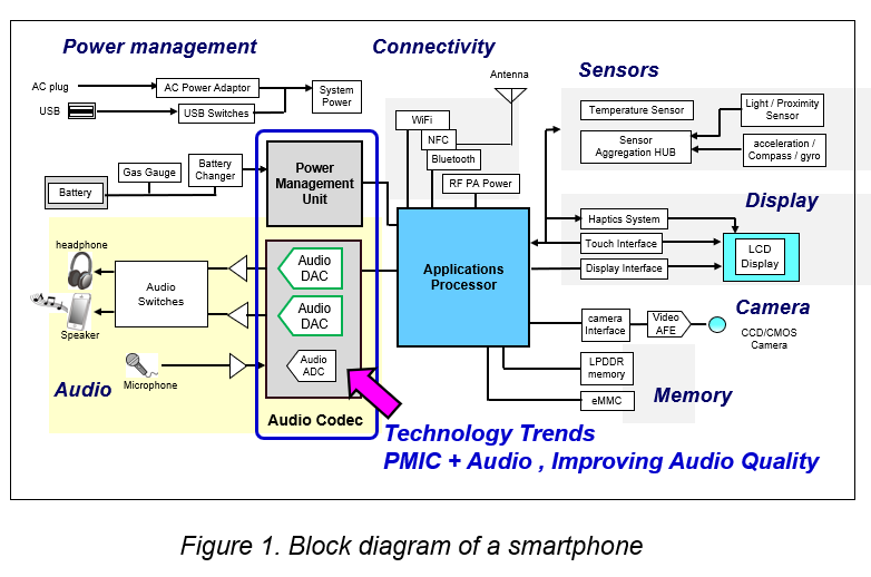
Figure 1 shows a block diagram of a smartphone. Smartphones incorporate numerous semiconductors to drive power management, connectivity, sensors, displays, audio, cameras, and memory. In recent years, there has been a trend toward integrating the PMIC and audio coder/decoder (CODEC) into a single chip, as the figure illustrates. There has also been an increase in 24-bit resolution DAC, needed for support of Hi-Res Audio.

What is Hi-Res Audio?

The Hi-Res Audio specification – defined by the Japan Electronics and Information Technology Industries Association (JEITA) – allows a much wider dynamic range than that provided by CDs. A Hi-Res sound source, such as 24 bit / 96 kHz or 24 bit / 192 kHz, is converted to data at a finer resolution than a CD sound source (Figure 2), so it has much more sound information compared to a CD sound source. This means that Hi-Res Audio is as close as possible to the original sound, enabling the listener to experience sound quality comparable to being in a studio or concert hall.

Audio testing

The four test methods required for audio devices are the tests for total harmonic distortion (THD); total harmonic distortion + noise (THD+N); dynamic range (DR); and signal noise ratio (SNR). Each of these tests determines various requirements associated with Hi-Res Audio, and together they create a set of parameters that must be met in order to assure the highest quality audio performance.

 Once these tests are completed, frequency weighting is used to obtain measurement values matching the sensitivity of the human ear. The frequencies people hear the best are in the range from 2 to 4 kilohertz (kHz), and sensitivity declines at frequencies that are higher or lower.

A-weighting is commonly used for the weighting network. SNR/DR tests often show analog performance when A-weighting is applied.

Measurement error occurs when measured noise can be calculated from the difference between device performance and measurement instrument performance. For example, if the difference between device performance and measurement instrument performance is 0 dB, the measurement error is 3 dB. If the difference is -5 dB, measurement error is 1.19 dB. This clearly indicates that the better the performance of the measurement instrument, the lower the measurement error.

Advantest solution

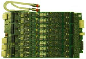
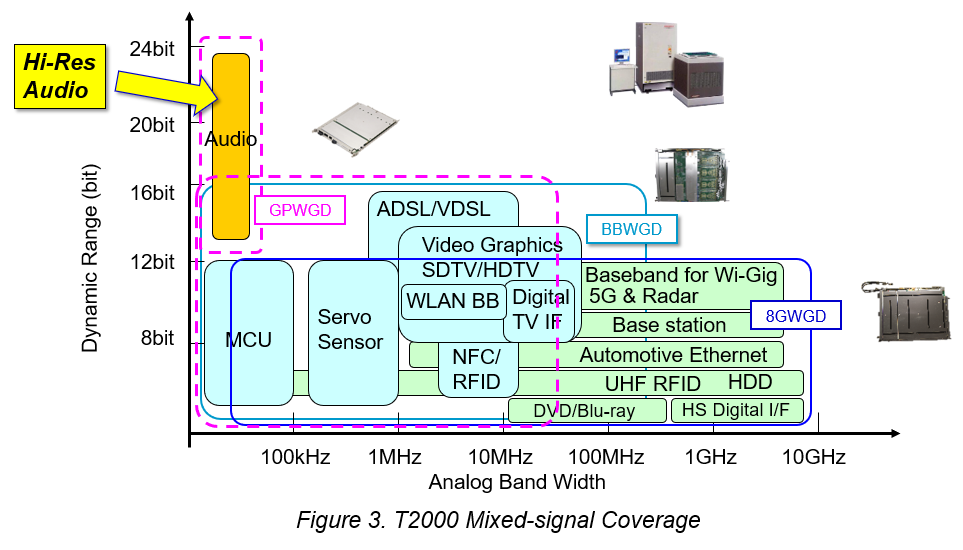
The T2000 supports three Mixed-signal modules (GPWGD, BBWGD,8GWGD) as shown in Figure 3.

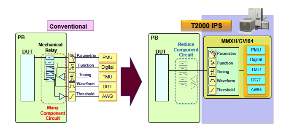
Advantest has developed a measurement technique with ultrahigh dynamic range to achieve industry-leading levels of analog performance for 24bit DAC solution, by adding high-precision analog circuits such as a band elimination filter (BEF) at the front-end of its T2000 general purpose waveform generator digitizer module (GPWGD).

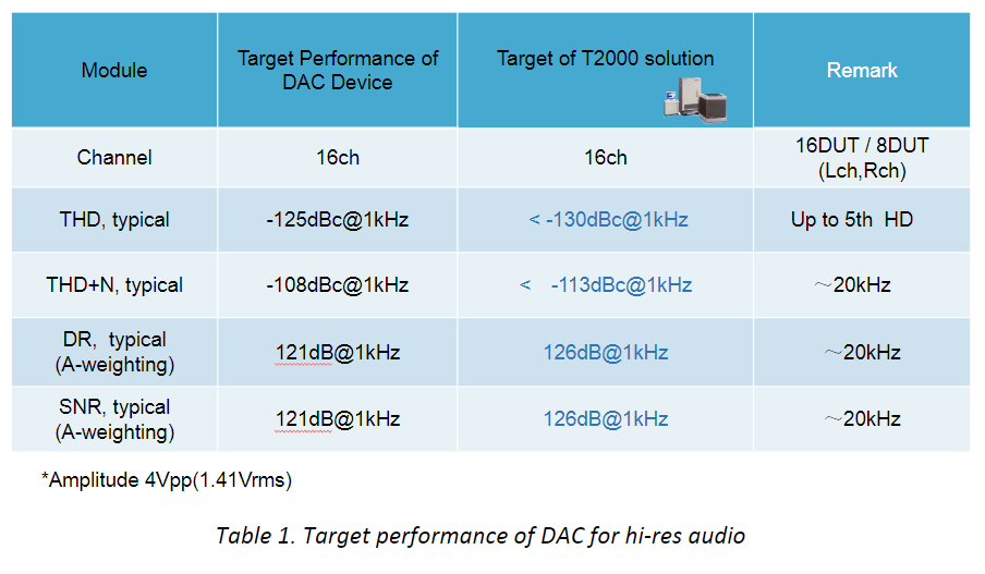
 The target performance for the T2000 solution was set to be 5dB better than target device performance in order to enable analog measurement with higher precision from characterization to mass production (Table 1). The test results performed indicated that the T2000 Integrated Power System (IPS) + GPWGD solution can address multiple challenges associated with Hi-Res audio testing, including high dynamic range measurement, power supply/GND design and isolation, high multi-site testing.

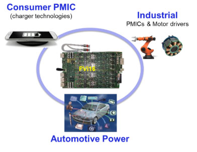
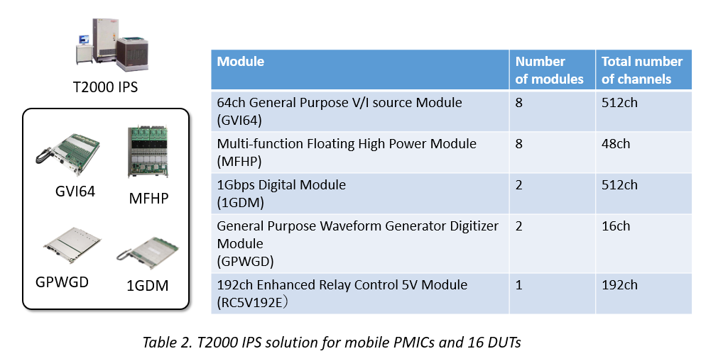
Mobile PMICs require digital, high-precision mixed-signal/analog, and power testing. As a product for automotive/industrial devices and PMICs, the T2000 IPS system can have a number of modules installed, as shown in Table 2. A high-precision analog function can also be added to the front-end of the GPWGD as a 24-bit DAC solution for Hi-Res Audio. For semiconductor manufacturing pre-processing, a wafer prober, probe card, and pogo tower can be combined together. The analog circuits can be equipped with 16 channels by mounting additional analog circuits in the user area on the wafer prober.

Measurement results

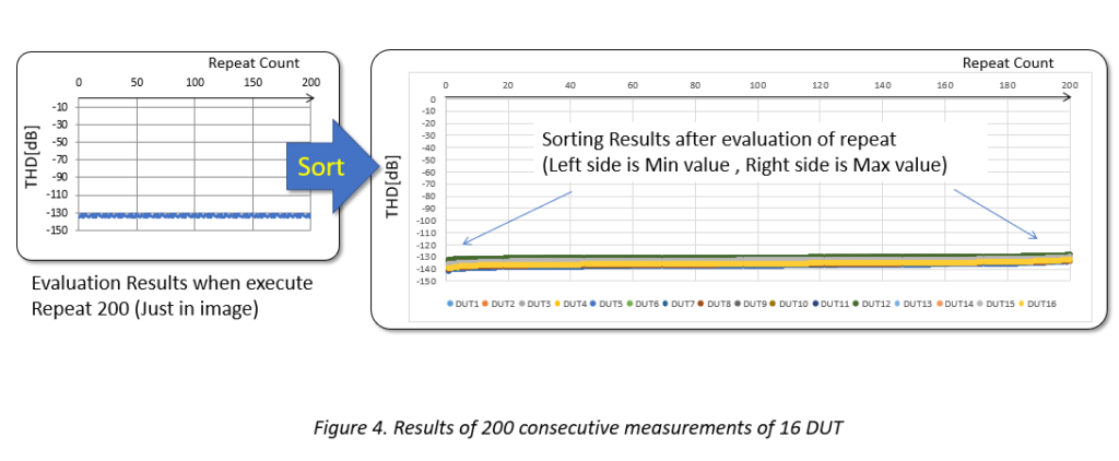
On the T2000 platform, analog performance was demonstrated with an ultra-high dynamic range, showing that the platform can achieve results beyond the target performance – as occurred when all of the audio tests listed earlier were conducted. Moreover, the results are consistent and repeatable, as indicated in Figure 4. When measurements were performed 200 times continuously with 16 multi-site tests, a typical THD result of -134 dBc was consistently obtained.

The results detailed in this article indicated that twice the number of multi-site tests can be achieved compared to conventional systems when the T2000 is combined with an IPS and GPWGD module. This makes it possible for the solution to support everything from characterization to mass production for PMICs associated with Hi-Res Audio. Future test efforts will take on the challenge of solutions for 32-bit DACs that require a higher dynamic range.

* dBc = decibels relative to the fundamental carrier power level; standard measurement for total harmonic distortion (THD)

Read More

Posted in Featured Products

Meeting Advanced Power and Analog Test Requirements

By Derek Floyd, Director of Business Development, Advantest America

The market for power and analog devices is showing strong, consistent growth. Market research firm IC Insights forecasts that revenues for analog products—including both general purpose and application-specific devices—will increase by a compound annual growth rate (CAGR) of 6.6% to $74.8 billion in 2022 from $54.5 billion in 2017. Power-management analog devices help regulate power usage to keep devices running more efficiently and longer, while the automotive application-specific analog market is the third-fastest growing of 33 IC product categories classified by the World Semiconductor Trade Statistics (WSTS).

With the heavy concentration in industrial and automotive applications, focusing the V93000 scalable platform on analog/power-management devices has proven a successful strategy for Advantest. In looking at where to target the next generation of floating power input voltage (VI) sources, a clear need was evident in three key market areas with high-power requirements: consumer power-management ICs (PMICs) for wireless charging of mobile phones and other smart products; industrial applications; and automotive power devices (see Figure 1).

Figure 1. Top high-power target markets

In the automotive market, the demand for high-quality test necessitates greater test accuracy and stability, together with faster test times and more multisite testing – all enabling reduced costs. At the same time, in the consumer space, higher performance and higher-power electronics are needed to support fast wireless charging, i.e., a great deal of current is quickly dumped into the battery. Advantest meets these requirements with its latest floating power VI source, the FVI16.

Introduced in May, the FVI16 source supplies 250 watts of high-pulse power and up to 40 watts of DC power. These parameters allow the source to enable sufficient power testing of latest-generation devices while conducting stable and repeatable measurements.

Figure 2 illustrates the target applications for the FVI16, with 35- to 150-watt applications being the “sweet spot” for its capabilities. Leading the pack in terms of volumes is fast, wireless charging and USB power delivery, followed by key markets in the automotive and industrial arenas. The growth of autonomous and electric vehicles and more electronic systems on board all new cars will drive continued high demand for automotive devices. The automotive space comprises a wide variety of applications requiring power in the 50-100W range – examples include buck/boost devices, window control, braking and other safety-oriented functions.

Figure 2. FVI16 strategic applications

Key FVI16 Characteristics

The FVI16 source delivers 40W of continuous DC power, as well as 250W of pulse power, on each channel with no interruption and no dropout. This is crucial for operation in high-power environments/applications, and provides a significant advantage compared to competitive offerings. The industry’s most advanced, accurate and highly integrated card, the FVI16 offers more capability on a per-channel basis and a significantly higher level of integration – not to mention twice as many channels as other available sources. In addition, all 16 channels can operate in pulse mode simultaneously, be ganged and/or stacked, and each channel can run either completely independent or completely parallel, depending the user’s application requirements.

Other key characteristics include:

  • 16 fully independent power VI channels (4Q, Kelvin)
    • -60V … +60V, 3A DC (40W) / 10A Pulse (250W)
    • 18-bit force/measurement accuracy ±200μV / ±10nA
    • Highly flexible and transparent
      • Ganging up to ±155A
      • Stacking up to ±180V
    • Floating range of ±200V
    • 18-bit 1 Msps AWG and digitizer (voltage and current)
    • SmartFeatures: Smart Connect/Range/Setting/Mode
    • Synchronous operation to other channels and digital “domain sync”
    • Fully pattern-controlled deterministic setup & measurement
  • 16 high-voltage VI: -60V … +120V, 30mA
  • 16 high-voltage time measurement units (TMU): -60V…+120V / 45MHz

The FVI16 is based on the core digital feedback loop (DFL; see Figure 3) of the existing AVI64 floating source, which has realized significant market success and will continue to compliment customers’ low-power testing requirements. Both systems feature best-in-class accuracy, while the DFL capability enables simultaneous measurement of voltage and current to provide instantaneous power monitoring, and comes with a number of smart features, as noted above, including glitch-free connection, range, and mode settings on the fly in order to prevent damage to devices.

Figure 3. FVI16 digital feedback loop diagram and benefits

Already in use at several customer sites, the FVI16 floating power VI source has generated multiple orders from leading automotive customers. Flexible licensing arrangements are available to allow customers to ensure the solution meets their specific needs.

Read More

Posted in Featured Products

Advantest’s Floating Power Source – the FVI16 – Extends V93000 Test Platform’s Capabilities in Diverse Power-Management Markets

Advantest has extended the performance of its V93000 single scalable platform with the FVI16 floating power VI source for testing power and analog ICs used in automotive, industrial and consumer mobile-charging applications such as the growing e-mobility and rapid charger market. By supplying 250 watts of high-pulse power and up to 40 watts of DC power, the new source helps to provide sufficient power testing latest generation devices while conducting stable and repeatable measurements.

The enhanced power resource gives the V93000 platform the industry’s best VI signal performance and expands its coverage into new markets, making it the broadest test solution available. With the FVI16, this versatile test platform is now equipped for testing semiconductors for a wider range of power-management devices, from airbags and ABS (anti-lock braking system) controllers to USB-C chargers and cordless power tools.

The system’s digital feedback loop design provides the best source, measurement accuracy and analog/power performance on the market, compared to competitors’ systems that operate with a traditional analog feedback. Digital feedback technology offers several unique features including spike-free “smart connections” with constant Kelvin monitoring for reliable and highly precise measurements. User-controllable slew rate and bandwidth settings allow fast settling times adapted to the respective load conditions.

The FVI16 unit features the industry’s highest instrument-channel density, enabling small system configurations that fit into Advantest’s A-Class test head and therefore lowers cost of test. Sixteen channels with four-quadrant operation allow for source ganging of up to 155 amps per card on high-current tests. For high-voltage testing, source stacking of up to +180 volts per card within a floating range of + 200 volts can be achieved.

The FVI16’s patented integrated fast current clamp protects the loadboard hardware, probe card pins and DUT sockets in case a damaged device creates a short circuit. Customers can use the new FVI16 to extend the capabilities of their existing V93000 Smart Scale systems to the higher voltages, increased channel count and power demands for high-site- count IC testing while maintaining a low cost of test.

Already in use at several customer sites, the FVI16 floating power VI source has generated multiple orders from leading automotive customers in Europe and Japan. Advantest is offering flexible licensing arrangements that allow customers to select the best fit for their specific needs.

FVI16

Read More

Posted in Featured Products

Advantest Extends its T2000 Product Line with Two New Modules Optimized for Testing High-Power Analog ICs Used in Electric Vehicles

Advantest has introduced two new modules that enable its T2000 IPS system to test high-voltage and high-power devices used in the power trains of electric vehicles (EV/HV).  The new enhanced MMXHE (multifunction mixed high voltage) and MFHPE (multifunction floating high power) modules enable massively parallel, high-performance testing by leveraging Advantest’s innovative multifunctional pin design, which allows unprecedented flexibility in assigning test resources to any pin.

The MMXHE and MFHPE modules optimize testing efficiency and lower the cost of test by providing 64 output channels and 36 output channels respectively.  Each pin has multiple measurement capabilities, which minimizes the number of relays on the loadboard for streamlined operation and a simpler loadboard design.

The modules can measure voltages up to 300 V with accuracy up to the order of 100 uV, as required in testing ICs in power trains, controls and sensors of EV/HVs.  Module resources can be stacked or ganged, giving customers the ability to adjust the tester’s functionality and throughput to achieve their desired performance.  This versatility helps to ensure the long-term usability of the T2000 IPS tester.

The system’s capabilities include highly accurate testing of parametric measurement units (PMU), high-voltage digital functions, differential voltages, time measurements, Iddq, and arbitrary waveform generator/digitizer functions.  With the T2000 IPS, each of these tests is assigned to a single pin, resulting in faster processing and higher throughput.

Read More

Posted in Featured Products

W2BI’s New MLT1600 Device Test Automation Platform Addresses LTE, GSM and WCDMA Capabilities for the Burgeoning IoT and Smartphone Markets

W2BI, an Advantest Group company and a global leader in wireless device test automation products for the world’s top wireless operators, suppliers and labs, has introduced the MLT1600 cloud-enabled, device test automation tester as the newest member of its Micro Line Tester portfolio. The MLT1600 addresses the testing challenges of IoT products across multiple cellular radio technologies – such as GSM, WCDMA and LTE – with a 70-MHz to 6-GHz frequency range. With its portable design and small footprint, the MLT1600 leverages W2BI’s existing cloud-based test management platform to acquire on-demand test cases and publish test results as required across all test parameters.

During Verizon’s Test Fest in Bridgewater, N.J., W2BI demonstrated the MLT1600 with multiple-use case scenarios, including device connectivity, VoLTE, IMS roaming, data performance, UICC and more. The system software includes commercial-grade eNodeB, EPC, IMS and built-in Web-App-FTP servers to provide end-to-end network emulation in support of automated testing to accelerate time to market with increased capacity.

As mobile devices continue to grow in number, they are becoming increasingly sophisticated and able to perform complex functions across all industries and consumer markets. Cellular networks, which span the globe with standardized mobile access and interoperability, are seeing a proliferation of IoT devices and applications. To ensure that devices and services remain highly reliable, wireless operators around the world need to ensure that new technologies meet the demands and the security requirements of the expanding IoT ecosystem.

To support this growth, W2BI is simplifying the testing process by offering MLT products that use multi-level intuitive reporting to enable rapid troubleshooting and root cause analysis of test failures. The results can be published over the cloud to allow remote log analysis. In addition, MLT test equipment automation products are expandable, easy to use and offer shorter test cycles with more comprehensive analysis.

W2BI is continually pursuing ways of lowering the cost of testing and making the technology accessible to all groups across the mobile ecosystem. The company is constantly expanding their test automation scripts that support mobile operator-specific and industry standards-based test specifications, such as 3GPP, Global Certification Forum and CTIA, to accelerate and simplify the testing process.


Read More

Posted in Featured Products

Five Key Success Factors for Automotive Device Test

By Kotaro Hasegawa, Senior Director, ADS System Planning Department, Advantest Corp.


The number of automotive-related semiconductor devices being designed into vehicles has been growing rapidly due to increased requirements associated with safety, in-vehicle entertainment, and advanced driver assistance systems (ADAS; see Figure 1). As ADAS content advances, we move closer to autonomous vehicle driving (Figure 2), which will require even more devices.

Figure 1. Automotive-related device market trends (Fuji Chimera Research Institute, Inc., 2017)

In turn, as this demand, goes up, production volumes for application-specific standard products (ASSPs) need to escalate. Thus, more cost-effective testing solutions are required to improve cost of test (COT) while maintaining test quality. Automotive devices must work all the time – this is a critical safety factor, made even more so in the ADAS era. Thus, maintaining high device quality in mass production is essential to developing automotive ASSP device test cells.

Below are five key factors associated with achieving testing success and helping ensure high quality as emerging automotive ASSPs enter into mass production.

Figure 2. Definition of ADAS levels (copyright SAE International, 2014)

1. Optimized Parallelism
Typically, when testing system-on-chip (SoCs) on automated test equipment, parallelism is mainly defined by resource counts. To increase the amount of parallelism, you simply add further resources onto the tester and align them with the prober or handler. Automotive ASSPs, however, involve a large amount of analog testing using an external control circuit due to the need to simulate an application model for high-quality testing. Performance board (loadboard) space is required to mount all components necessary for testing the device under test (DUT).

In many cases, even with sufficient resources on the test head, loadboard space limitations prevent achieving the desired level of parallelism, which, in turn, limits productivity. One way to address this challenge is to expand the printed circuit board (PCB) area to ensure enough space is available to mount all components, but sometimes even this step is not sufficient.

The Advantest T2000 test platform incorporates two capabilities that address these parallelism limitations, allowing it to achieve greater parallelism than competitive platforms:

  • Reduction in application relays on loadboard – up to 40 percent fewer in some cases – provided by the T2000’s multifunctional modules (Figure 3).
  • Wider PCB support with RECT550EX fixture (HIFIX) – this feature can enable a 140-pin automotive ASSP device to expand x4 DUT testing to x8 DUT testing, as an example (see Figure 4).

Figure 3. Example of T2000 relay reduction multifunctional module


Figure 4. T2000 RECT550EX fixture (HIFIX)

2. Reduced Test Time
Once devices enter high-volume manufacture, test-time reduction becomes even more critical. The T2000 includes some unique features to improve productivity while maintaining test quality, enabling best-in-class performance.

Typically, test systems require the user to power off, change mode, and power on again, but this takes a great deal of time. The T2000 architecture’s switching methodology reduces power spikes by enabling mode switching during test. This reduced switching time is ideal for devices that are extremely COT and time-to-market (TTM) sensitive, such as automotive ASSPs.
Another testing method is to monitor the output behavior of the DUT. With the T2000, the hardware module can automatically detect the device output, and if there is any change in device state, the module can halt the arbitrary waveform generator’s (AWG) input as needed and assess the test result, then immediately move on to the next test item (see Figure 5). This capability speeds the process because waiting to receive the full-scale AWG output isn’t necessary.

Figure 5. Test time reduction method on AWG

3. Wide Coverage
The T2000 features 52 test head slots, allowing a reach of more than 8,000 digital and 6,400 analog channels. This lets the user obtain the best resourcing fit, choosing from wide variety of T2000 modules available. In addition, the T2000 can deliver both high voltage (up to 2000 V) and current (up to 216 A). With this wider coverage, the platform can be utilized to test automotive ASSPs, power management integrated circuits (PMICs), light-emitting diode (LED) drivers, and other devices with high resource requirements (see Figure 6).

Figure 6. The T2000’s test segment coverage is among the industry’s widest

4. Test quality
Advantest integrated into the T2000 platform a long lifecycle, as well as testing stability, accuracy and reliability. The platform and modules possess unique hardware/software design rules in order to achieve high-quality hardware. All modules are developed based on these design rules, including selection of the ICs for the module, to help ensure high system quality and reliability. These are key factors for testing quality-sensitive devices such as automotive ASSPs.

5. Field Proven
It takes a long time to launch new automotive-related devices into the market, and the test process is highly sensitive to changes in the production environment. Selecting a proven platform that includes all necessary capabilities is key to optimal testing of automotive-related devices. In addition, newer devices targeting this market will be highly integrated to include more functionality, voltage coverage, current, and frequency. In addition to being field-proven, the test system implemented will need to offer the widest coverage so that it is flexible and extendible.

Worldwide, more than 3,900 T2000 modules designed especially for automotive ASSP testing are already installed, and further growth is expected as the market for these devices continues to expand.

Given its combination of high-quality test, high productivity and widest device segment coverage, the T2000 is well suited for testing automotive and other quality-sensitive devices.


Read More